Compound Semiconductor
We contribute to the development of a society
with dreams, through cutting-edge
technology and reliable service.


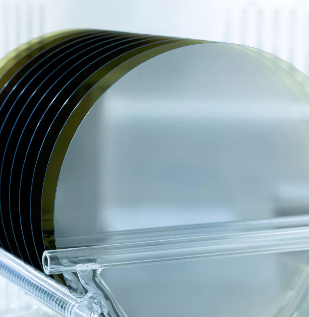
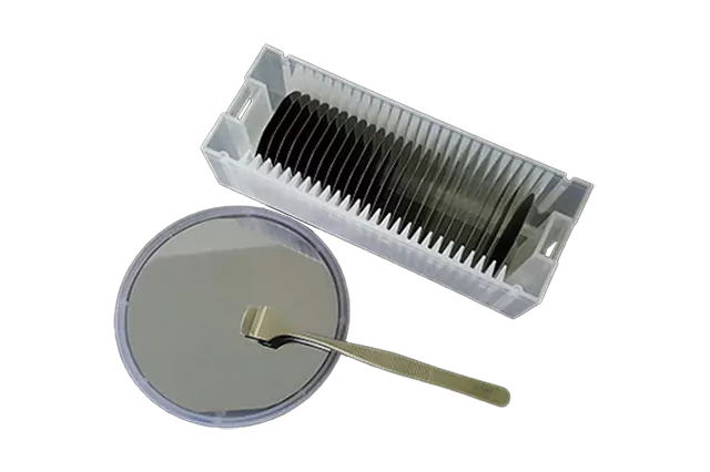
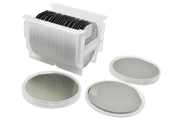
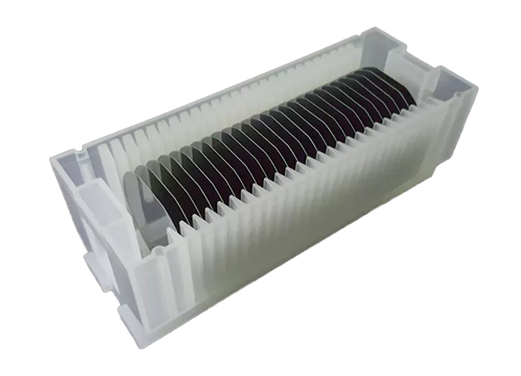
TOYOKOU CHEMI provides high-quality semi-insulating and semiconductor products such as gallium hydride, germanium, and indium phosphide substrates.
The electrical properties can be adjusted according to customer requirements.
In the crystal growth process, the type of conductivity (N-type or P-type) and electrical property parameters of the crystal are controlled by adjusting the doping and concentration.
Doping uses elements such as carbon (C), silicon (Si), iron (Fe), sulfur (S), and zinc (Zn).
Using the latest high-precision wire cutting equipment and high-precision plane grinding equipment, the wafer substrate is finished to a high-precision plane.
We provide high-quality epitaxial wafers, going through the CMP polishing process, cleaning process, and packaging process under strict quality control.

Gallium Arsenide (GaAs) Wafer Substrate
We provide 2 to 6 inch Gallium Arsenide (GaAs) substrates.
We have semi-insulating Gallium Arsenide (GaAs) with no additives, semiconductor Gallium Arsenide with Si additions, and Gallium Arsenide with Zn additions available.

Indium Phosphide (InP) Wafer Substrate
We provide high quality 2 to 4 inch Indium Phosphide (InP) wafers.
We offer products that include undoped, iron-doped, sulphur-doped, and zinc-doped, which are mainly used in the microelectronics and information communication fields.

Germanium Wafer Substrate
We provide 4 and 6 inch Germanium substrates.
We have products with electrical resistivity ranging from 0.05Ω·cm and above, including high resistivity products of 50Ω·cm and more.