GaN Wafer
We provide GaN wafer products.
- Accepts small orders
- Notable for use in power LSI, high-brightness LEDs, and lasers
- High quality (few crystal defects)
- Low price (compared to other companies)

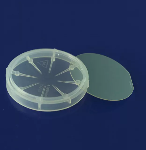
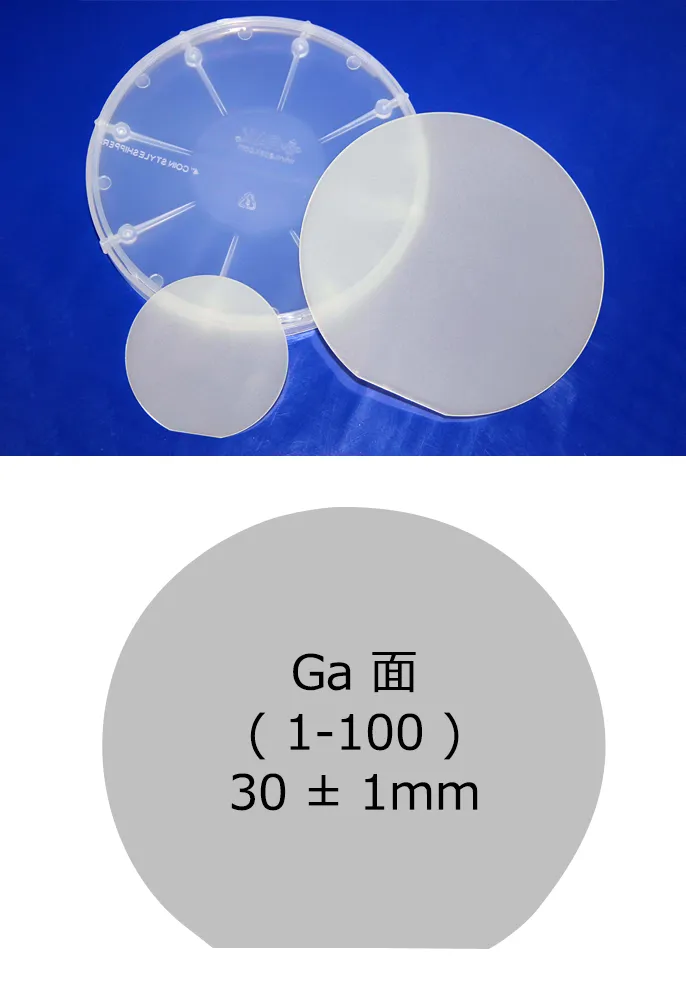
We also handle 1 to 2-inch GaN substrates.
GaN Substrate

| Item | Specification | ||
|---|---|---|---|
| Diameter | 51.0 mm ± 0.3 mm | 100.2 mm±0.3 mm | |
| Thickness | 490 µm ± 30 µm | 540 µm ± 30 µm | |
| Plane Orientation | (0001) Ga-Face c-plane | ||
| TTV (5 mm edge exclusion) | ≤15 µm | ≤30 µm | |
| Warp (5 mm edge exclusion) | ≤20 µm | ≤80 µm | |
| Bow (5 mm edge exclusion) | -10 µm to +5 µm | -40 µm to +20 µm | |
| Electrical Characteristics | Type | Resistivity | |
| N-type (Si) | ≤0.02 Ω·cm | ||
| UID | ≤0.2 Ω·cm | ||
| Semi-Insulating (Carbon) | >1E8 Ω·cm | ||
| Grade | Density (pits/cm2) | 2" (pits) | 4" (pits) |
| Production | ≤0.5 | ≤10 | ≤40 |
| Research | ≤1.5 | ≤30 | ≤120 |
| Dummy | ≤2.5 | ≤50 | ≤200 |
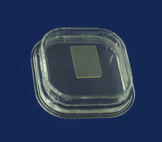
GaN Substrate (Square)
| Item | Specification | ||
|---|---|---|---|
| Size | (10 ± 0.5) × (15 ± 0.5) mm2 Customized Size |
||
| Thickness | 400 ± 25 µm | ||
| Plane Orientation | C-plane (0001) off-angle toward M-axis 0.35 ± 0.15° or 0.55 ± 0.15° |
||
| TTV | ≤10 µm | ||
| BOW | ≤10 μm | ||
| Type | UID | N-type (Si) | Semi-Insulating (Carbon) |
| Ga face surface roughness | <0.3 nm (10 × 10 μm) | ||
| N face surface roughness | Etched (0.5–1.5 µm); Polished (<0.3 nm) | ||
| Dislocation Density | <1 × 106 cm-2 | ||
| (002) FWHM | ≤70 arcsec | ||
| (102) FWHM | ≤70 arcsec | ||
| Macro defect density(hole) | <0.3 cm-2 | ||
| Effective Area | >90% | ||
GaN Template (φ2 inch)

| Item | Specification | |
|---|---|---|
| Diameter | φ50.8 mm ± 0.1 mm | |
| GaN Film Thickness | 4 µm, 10–25 µm | |
| Oriented Plane | C-plane (0001) ± 0.5° | |
| Type | UID | N-type (Si) |
| Orifura Orientation. Length | Orifura orientation (1-100). Orifura length 30 mm ± 1 mm | |
| Electrical Resistivity (300 K) | <0.5 Ω·cm | <0.05 Ω·cm |
| Dislocation Density | 5 × 108 cm2 | |
| Substrate Structure | GaN/Sapphire Wafer (0001) Surface | |
| Effective Area | More than 90% | |
| Surface Finish | Ga side: CMP finish. N side: Fine grinding (Option: Optical mirror finish) | |
GaN Template (φ4 Inches)
| Item | Specification |
|---|---|
| Diameter | φ100 mm ± 0.1 mm |
| GaN Film Thickness | 4 µm, 10–25 µm |
| Oriented Plane | C-plane (0001) ± 0.5° |
| Conductivity Type | N-type (Undoped) |
| Orifura Orientation. Length | Orifura orientation (1–100). Orifura length 30 mm ± 1 mm |
| Electrical Resistivity (300 K) | <0.5 Ω·cm |
| Dislocation Density | 5 × 108 cm2 |
| Substrate Structure | GaN/Sapphire Wafer (0001) Surface |
| Effective Area | More than 90% |
| Surface Finish | Ga side: CMP finish. N side: Fine grinding (Option: Optical mirror finish) |
Power Using GaN-on-Si Epitaxial Wafer
| Items | Values/Scope |
|---|---|
| Wafer Diameter | 100mm, 150mm, 200mm, 300mm |
| Substrate | Si |
| Epi-layer Thickness | 2 ~ 7 μm |
| EWafer Bow | <30 μm, Typical |
| Surface Morphology | RMS < 0.5 nm (5 × 5 μm2) |
| Barrier | AlXGa1-XN (0 < x < 1) |
| Cap Layer | In-situ SiN or GaN (D-mode); p-GaN (E-mode) |
| 2DEG Density | >9E12/cm2 (20nm Al0.25GaN, 150mm) |
| Electron Mobility | >1800 cm2/Vs (20nm Al0.25GaN, 150mm) |
- Features
-
- Excellent device performance enabled by high electron mobility and high 2DEG density
- Low bow for superior process compatibility
- Support for large diameters (up to 300 mm) for improved mass production capability
- Compatible with both D-mode and E-mode structures
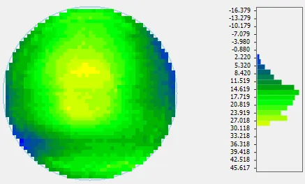
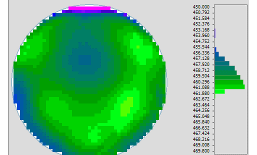
200mm GaN-on-Si Epiwafer
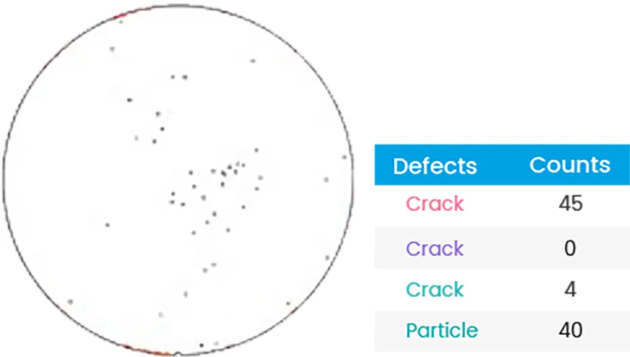
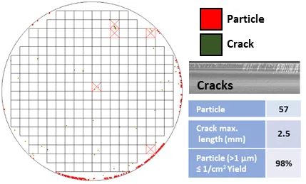
Defect Mapping
Vertical Breakdown Behavior
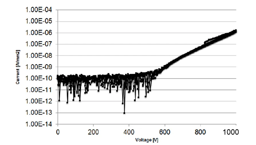
Sheet Resistance Mapping
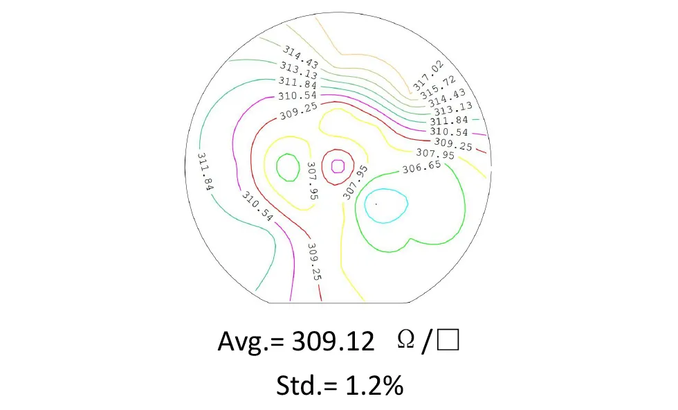
Wafer Bow Mapping
GaN Epitaxial Wafer for Micro LED
| Items | GaN-on-Si | GaN-on-Sapphire |
|---|---|---|
| 100mm, 150mm,200mm, 300mm | 50.8mm, 100mm, 150mm | |
| Epi-layer Thickness | <4 μm | <7 μm |
| Average Dominant/Peak Wavelength | 400–420 nm (near UV) | 270–280 nm (UVC) |
| 440–460 nm (Blue) | 440–460 nm (Blue) | |
| 510–530 nm (Green) | 510–530 nm (Green) | |
| - | 620–640 nm (Red) | |
| FWHM | <25nm for Blue/Near-UV <45nm for Green |
<15nm for UVC <25nm for Blue <40nm for Green |
| Wafer Bow | <50 μm | <180 μm |
- Features
-
- Supports a wide wavelength range from UVC to visible light (red)
- Compatible with large-diameter GaN-on-Si wafers (up to 300 mm)
- Excellent luminescence characteristics achieved through high-quality epitaxial growth
- High uniformity and high-precision epitaxial structure suitable for Micro LED applications
200mm GaN-on-Si Epiwafer for Micro-LED
DDominant Wavelength
Avg: ~450 nm, Std<2 nm
Avg: ~450 nm, Std<2 nm
TDD: <1e9 cm-2
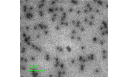
Defect Inspection
GaN-on-GaN Epitaxial Wafer
- Size: 2 to 4 inches
Epitaxial Wafer for RF Applications
- GaN-on-Si: 4 to 8 inches
- GaN-on-SiC: 2 to 6 inches
- In-situ SiN/Al(In)N/GaN heterostructure
The size, epitaxial structure, film thickness, etc., can be customized according to your requirements.
Detailed specifications can be optimized based on your requests.