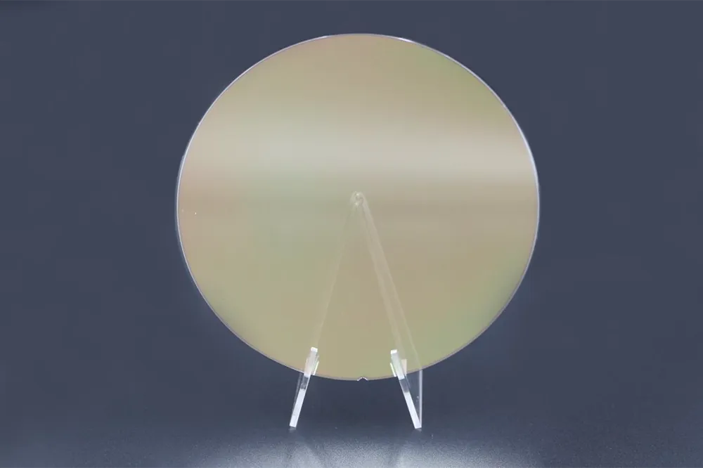
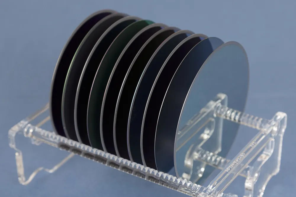
Composite Wafer
N-type SiC Composite Wafer

| Item | Specification | Item | Specification |
|---|---|---|---|
| Diameter | 150 ± 0.2 mm | Front (Si-face) roughness | Ra ≤ 0.2 nm (5 μm × 5 μm) |
| SiC Type | 4H | Edge Chip, Scratch, Crack (visual inspection) | None |
| SiC Resistivity | 0.015–0.025 Ω·cm | TTV | ≤3 μm |
| Transfer layer Thickness | ≥0.4 μm | Warp | ≤35 μm |
| Void | ≤5 ea/wafer (2 mm > D > 0.5 mm) | Thickness | 350 μm ± 25 μm |
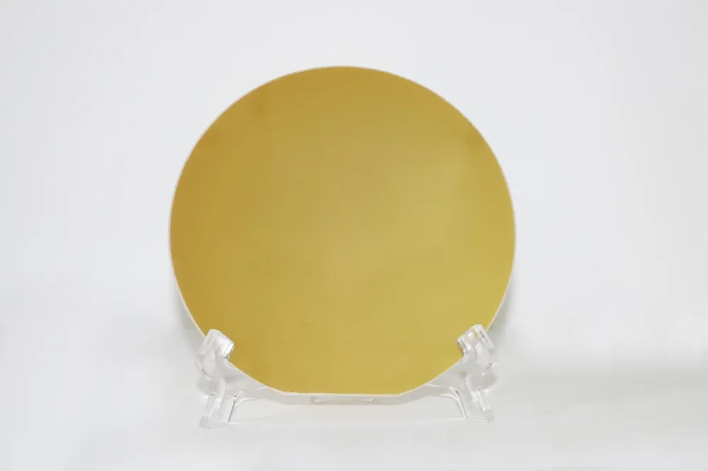
Semi-insulating SiC Composite Wafer

| Item | Specification | Item | Specification |
|---|---|---|---|
| Diameter | 150 ± 0.2 mm | Front (Si-face) roughness | Ra ≤ 0.2 nm (5 μm × 5 μm) |
| SiC Type | 4H | Edge Chip, Scratch, Crack (visual inspection) | None |
| SiC Resistivity | 0.015–0.025 Ω·cm | TTV | ≤3 μm |
| Transfer layer Thickness | ≥0.4 μm | Warp | ≤35 μm |
| Void | ≤5 ea/wafer (2 mm > D > 0.5 mm) | Thickness | 500 ± 25 μm |
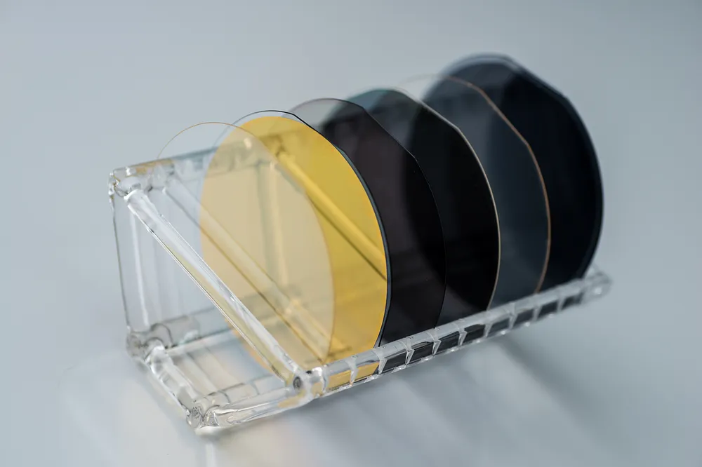
N-type SiC on Si Composite Wafer

| Item | Specification | Item | Specification |
|---|---|---|---|
| Diameter | 150 ± 0.2 mm | Si Orientation | <111>/<100>/<110> |
| SiC Type | 4H | Si Type | P/N |
| SiC Resistivity | 0.015–0.025 Ω·cm | Flat length | 47.5 ± 1.5 mm |
| Transfer SiC layer Thickness | ≥0.1 μm | Edge Chip, Scratch, Crack (visual inspection) | None |
| Void | ≤5 ea/wafer (2 mm < D < 0.5 mm) | TTV | ≤5 μm |
| Front roughness | Ra ≤ 0.2 nm (5 μm × 5 μm) | Thickness | 500/625/675 ± 25 μm |
Semi-insulating SiC on Si Composite Wafer

| Item | Specification | Item | Specification |
|---|---|---|---|
| Diameter | 150 ± 0.2 mm | Si Orientation | <111>/<100>/<110> |
| SiC Type | 4H | Si Type | P/N |
| SiC Resistivity | ≥1E8 Ω·cm | Flat/Notch | Flat/Notch |
| Transfer SiC layer Thickness | ≥0.1 μm | Edge Chip, Scratch, Crack (visual inspection) | None |
| Void | ≤5 ea/wafer (2 mm > D > 0.5 mm) | TTV | ≤5 μm |
| Front roughness | Ra ≤ 0.2 nm (5 μm × 5 μm) | Thickness | 500/625/675 ± 25 μm |
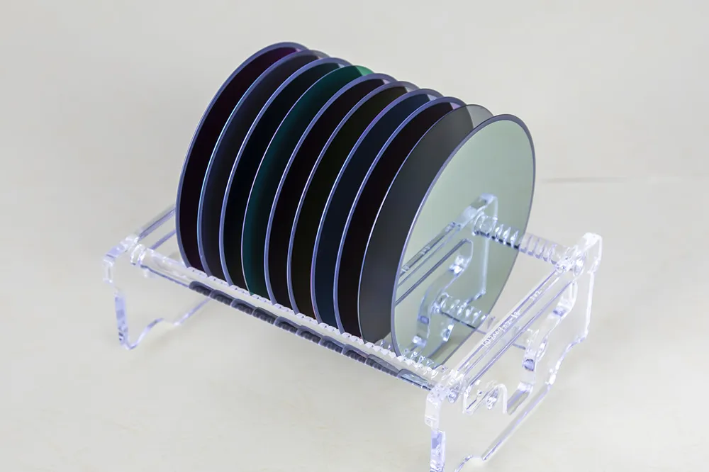
Si on SiC Composite Wafer

| Item | Specification | Item | Specification |
|---|---|---|---|
| Diameter | 150 ± 0.2 mm | SiC Type | 4H |
| Si Orientation | <111>/<100>/<110> | SiC Resistivity | 0.015–0.025/≥1E8 Ω·cm |
| Si Type | P/N | Flat/Notch | Flat/Notch |
| Transfer Si layer Thickness | ≥0.1 μm | Edge Chip, Scratch, Crack (visual inspection) | None |
| Void | ≤5 ea / wafer (2 mm > D > 0.5 mm) | TTV | ≤5 μm |
| Front roughness | Ra ≤ 0.2 nm (5 μm × 5 μm) | Thickness | 350/500 ± 25 μm |
Si on AlN Composite Wafer

| Item | Specification | Item | Specification |
|---|---|---|---|
| Diameter | 150 ± 0.2 mm | AlN Resistivity | ≥1E8 Ω·cm |
| Si Orientation | <111>/<100>/<110> | AlN Thermal conductivity | ≥180 W/m·K |
| Si Type | P/N | Flat length | 47.5 ± 1.5 mm |
| Transfer Si layer Thickness | ≥0.1 μm | TTV | ≤5 μm |
| Edge Chip, Scratch, Crack (visual inspection) | None | Thickness | 625 ± 25 μm |
| Front roughness | Ra ≤ 0.2 nm (5 μm × 5 μm) |
SOI Wafer
| Size | inch | 4 | 5 | 6 | 8 | 12 |
|---|---|---|---|---|---|---|
| Active Layer | Unit | Specification | ||||
| Manufacturing Method | - | CZ/FZ | ||||
| Type / Conductivity | - | P/N/Non-doped | ||||
| Crystal Orientation | - | <100>/<111>/<110> | ||||
| Dopant | - | B, P, As, Sb | ||||
| Thickness | μm | ≧1.0 | ||||
| *Resistivity | Ω·cm | 0.001–10000 | ||||
| *Embedded Oxide Film | μm | 0.05–10 | ||||
| Support Substrate | Specification | |||||
| Manufacturing Method | - | CZ/FZ | ||||
| Type / Conductivity | - | P/N/Non-doped | ||||
| Crystal Orientation | - | <100>/<111>/<110> | ||||
| Dopant | - | B, P, As, Sb | ||||
| *Thickness | μm | JEITA・SEMI Standard/200-1500 | ||||
| *Resistivity | Ω·cm | 0.001–10000 | ||||
| Remarks | *Please inquire separately for detailed specifications. | |||||
300-900nm LiNbO3 Single Crystal Thin Film (LNOI)

● Lithium Niobate Thin Film
● SiO2
● Si, LN, Quartz, Fused Silica, etc.
| Top Functional Layer | Diameter | 3, 4, (6) inches | Orientation | X, Z, Y, etc. |
|---|---|---|---|---|
| Material | LiNbO3 | Thickness | 300-900 nm | |
| Doping (Optional) | MgO | |||
| Separation Layer | Material | SiO2 | Thickness | 1000-4000 nm |
| Substrate | Material | Si, LN, Crystal, Fused Quartz, etc. | ||
| Thickness | 400-500 μm | |||
| Optional Electrode Layer | Material | Pt, Au, Cr | Thickness | 100-400 nm |
| Structure | Above or below the SiO2 separation layer | |||
300-900nm LiTaO3 Single Crystal Thin Film (LTOI)
● Lithium Tantalate Thin Film
● SiO2
● Silicon
| Top Functional Layer | Diameter | 3, 4, 6 inches | Orientation | Y-42, Y-46.3, Z, etc. |
|---|---|---|---|---|
| Material | LiTaO3 | Thickness | 300-900 nm | |
| Separation Layer | Material | SiO2 | Thickness | 300-4000 nm |
| Substrate | Material | Si | ||
| Thickness | 400-500 μm | |||
5-50μm LT & LN thin film on Si substrate

● Lithium Tantalate Thin Film
● Silicon
● Lithium Niobate Thin Film
● SiO2
● Silicon, Quartz, etc.
| Top Functional Layer | Diameter | 3, 4, 6 inches | Orientation | Y-42, Y-46.3, Z, etc. |
|---|---|---|---|---|
| Material | LiTaO3 | Thickness | 300-900 nm | |
| Separation Layer | Material | SiO2 | Thickness | 300-4000 nm |
| Substrate | Material | Si | ||
| Thickness | 400-500 μm | |||
20-60μm ultra-thin, super flat wafer

● Lithium Tantalate Thin Film Or Lithium Niobate Thin Film
| Diameter | 3, 4 inches | Orientation | X, Y, Z, etc. |
| Thickness | 10-60 μm | Material | LN, LT, Si, etc. |
| Surface | Double-sided or single-sided polishing | ||
Custom-made LN & LT thin film
| Top Layer/Details | Substrate Details | Top Layer Thin Film Details | ||||||
| Multilayer Structure | Electrode & Waveguide Pattern | Different Materials (SiO2/Si, Si, Sapphire, Quartz, etc.) | PPLN | Special Sizes | Electrodes (Au, Pt, Cr, Al, etc.) | Orientation (same as bulk wafer) | Doping (MgO, Fe, Er, Tm, etc.) | |
| 100-1000 nm LiNbO3 | √ | √ | √ | √ | √ | √ | √ | √ |
| 100-1500 nm LiTaO3 | √ | √ | √ | √ | √ | √ | √ | |
| 5-50 μm LiNbO3 | √ | √ | √ | √ | ||||
| 5-50 μm LiTaO3 | √ | √ | √ | √ | ||||