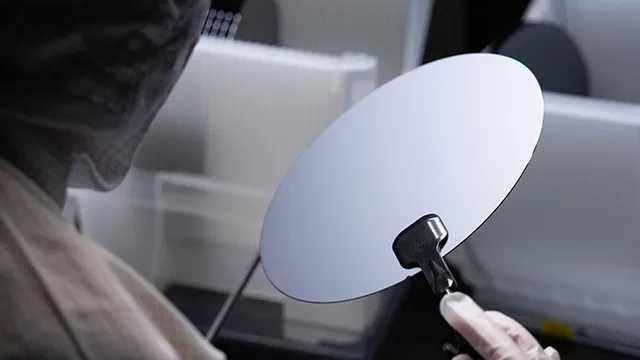
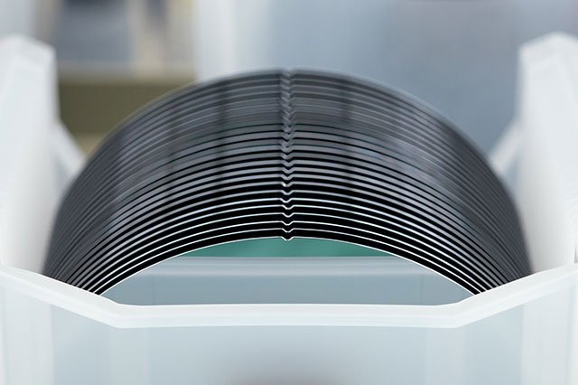
Silicon Wafers
We provide silicon wafers used as semiconductor substrates ranging from 2 inches to 12 inches, depending on customer's application and requests.
We have wide selection of products from major manufacturers, and we can propose wafers that are optimal for applications and plans of various manufacturers, universities, and research institutes.
We stably supply wafers of reliable quality that meet customer requests.
| Item | Unit | Specifications | ||||||
|---|---|---|---|---|---|---|---|---|
| Size | Inch | 2 | 3 | 4 | 5 | 6 | 8 | 12 |
| Thickness | μm | 280 ± 25 | 380 ± 25 | 525 ± 25 | 625 ± 25 | 625 ± 25 | 725 ± 25 | 775 ± 25 |
| Crystal Growth | - | CZ/FZ | ||||||
| Crystal Orientation | - | <100>/<111>/No Preference | ||||||
| Type | - | P/N/No Preference | ||||||
| Resistivity | Ω·cm | 0.01-1,000 | ||||||
| Surface Finish | - | Single-Sided / Double-Sided Mirror | ||||||
| Packing Form | - | Coin Roll/Cassette Case | ||||||
ST Wafer (Power Semiconductor Substrate)
Product Information
[ST wafer] is a single crystalized wafer that improved mechanical strength by doping B and Ge during the manufacturing process.
The characteristics are strong anti-heat shock in high-temperature process and exemplary performance in reducing slips and warp value for hetero-epitaxial growth such as GaN.
Product Specification
- Diameter: 4,5,6 inch
- Dopant: B-Ge (P type)
- Crystal Orientation: <111>
- Resistivity: ≤0.02 Ωcm
Main Application
- GaN-on-Si (Power Semiconductor Substrate)
Ultra High Flatness Wafer
Product Information
STC has succeeded in manufacturing single crystal silicon substrate, which has a high flat value even in small diameter. Usually, the limit of TTV is around 3μm in small diameter, but STC has exceeded its limit and accomplished better than 1μm. STC will also apply better flatness quality as per the customer’s requirements.
Ultra-High Flatness Wafer can be used for the base substrate, which is applicable for bonding or photolithography processes, and will fit for good uniformity based on several deposition processes, which means proper substrate for accuracy demanded several devices.
Standard Products Spec
- Dia: 4, 6 inch
- TTV: ≤1 μmm (Actual: ≤0.5 μm)
- Type: P(B), N(Phos,Sb), FZ
- Orientation: <100>, <110>, <111>
- Resistivity: ≤0.005 ~ 40 Ωcm
- Finish: SSP, DSP
Main Application
- Substrate for bonding (SOI・LT・TC-SAW etc)
- Substrate for Photo-Lithography
- Process which needs good TTV as important parameter.
Effective Case
- To reduce time and cost for thinning, also to be good flatness to substrates for bonding
- To improve the yield rate of wafer outer area to the edge
Process Specification
| Items | 4 inch | 6 inch |
|---|---|---|
| Diameter (mm) | 100 ± 0.2 | 150 ± 0.2 |
| Thickness (μm) | 220~1300 ± 2 | 280~1300 ± 2 |
| Dopant (Resistivity) | B (0.005~40Ω), Phos (0.1~40Ω), Sb (0.01~0.1Ω), nondopantFz (≧1000Ω) | |
| TTV (μm) | ≦1 (Actual: ≦0.5μm) | ≦1 (Actual: ≦0.5μm) |
| LTV (μm) | ≦0.3 □ × 10 mm | ≦0.3 □ × 10 mm |
| Particles on front side | ≦10 Pieces (≧0.3μm) | ≦10 Pieces (≧0.3μm) |
| Surface Finish | Single-Sided / Double-Sided Mirror | Single-Sided / Double-Sided Mirror |
※ Other options. Please ASK.
- Enlarge diameter (101,151mm) for SOI terrace free.
- Additional oxide layer process for BOX layer
- Notch type instead of flat shape
- Non Dope ≥1000Ω (FZ)
Far-infrared Material - HT Silicone
HT silicone is a silicon material that has improved transmittance in the far-infrared region, particularly around 9 μm.
Product Information
- Crystal Growth: CZ Method
- Diameter: 4, 5, 6, (8) inch
- Resistivity: ≥180 Ωcm
- Oxygen Concentration: ≤8.0×10¹⁵ atoms/cm3
- Polycrystal
Product Shape
STC can provide the polished wafer (PW) product, as a lapped wafer (LW), like a sliced wafer, or even by ingot base.
Special Customization
As per the customer's requests, STC applies to provide by lens or window material shape with Anti-reflective (AR) coating or Diamond-like carbon (DLC) coating.
Silicon Ingot
Product Description
- Using manufacturing method called the CZ method (Czochralski method), we manufacture single crystal ingots, which are material for silicon wafers.
- This ingot is very important consumable material used primarily in etching process, which is one of device manufacturing processes.
- We can provide silicon ingot products in various sizes and resistivities according to customer requirements.
| Diameter (mm) | Type | Crystal Orientation | Purity | Resistance Value (Ω·cm) | Length |
|---|---|---|---|---|---|
| φ200-φ550 | P | <100>/<111> | 10-11 N | ≤0.01 | Custom-made |
| 1-4 | |||||
| 60-90 | |||||
| Custom-made |
Dummy Wafer
Strengths
- Wide range of products
- We carry wide variety of silicon wafers.
- Small lots available
- We can respond to customer requests with care and detail.
- Short delivery times
- We utilize our abundant inventory to provide products in short delivery times.
- Flexible response
- We can also process from ingots for standards that cannot be covered with stock wafers
We can process ingots even for specifications that are not in stock.
Through careful interviews with our customers, we propose optimal wafer that meets their needs. We can also ship in a format according to your request, such as in cassette case or coin roll case. Furthermore, we can sell wafers of any type or thickness at low cost.
Features
Because they are often used in experiments and tests, dummy wafers come in wide variety of sizes and thicknesses. In some cases, reclaimed wafers may also be used.
Compared to particle-controlled silicon wafer products, dummy wafers are cheaper and can be shipped in small lots. This is major feature of dummy wafers.
In manufacturing equipment, dummy wafers are sometimes used for first few wafers to improve process stability. It is also used to optimize and monitor manufacturing processes. Although dummy wafers are not suitable for device manufacturing, they exhibit sufficient performance for monitoring and testing purposes, and are widely used as replacement for new wafers.
Dummy wafers are indispensable and play important role in testing and adjustment in each process of wafer manufacturing.
| Item | Specification | ||||||
|---|---|---|---|---|---|---|---|
| Size | 2 | 3 | 4 | 5 | 6 | 8 | 12 |
| Crystal Growth | CZ/FZ | ||||||
| Type | P-type/N-type/No Preference | ||||||
| Crystal Orientation | <100>/<111>/<110>/No Preference | ||||||
| Notch/Off Orientation | <100>/<111>/<211>/No Preference | ||||||
| Thickness (μm) | 280 | 380 | 525 | 625 | 625/675 | 725 | 775 |
| Thickness Tolerance (μm) | 20 | 20 | 25 | 25 | 25 | 25 | 25 |
| Resistivity (Ω·cm) | 0.005~/No Preference | ||||||
| Olyfla | Olyfla | Olyfla | Olyfla | Olyfla | Notch/Olyfla | Notch/Olyfla | Notch |
| Surface Finish | Single-Sided / Double-Sided Mirror | Single-Sided / Double-Sided Mirror | |||||
| Particle | No Preference | ||||||
| Quantity | Orders are accepted from 25 pieces. | ||||||
| Packaging Type | Coin Roll/Cassette Case | ||||||
| Remarks | The 6-inch OriFla standard can be adapted to both JEITA and SEMI. | ||||||
Recycled Wafer
We utilize cutting-edge equipment along with high-standard chemical processing, polishing, and cleaning technologies to provide high-quality recycled wafers ranging from 8-inch to 12-inch sizes.
Recycled wafers refer to wafers that have been used as dummy/test wafers for equipment calibration and testing purposes in semiconductor manufacturing processes. These wafers are cleaned to remove contaminants, re-polished, and re-cleaned, making them reusable for repeated applications.
Half-inch Wafers (φ12.5 mm)
Overview
Half-inch wafers with a diameter of φ12.5 mm (approx. 0.5 inch) are ideal for research and development, laboratory experiments, process evaluation, and small-lot production.
Specifications
| Item | Description |
|---|---|
| Product | Diameter φ12.5 mm, thickness 0.25 mm |
| Si (100) Wafer: N-type, P-type | |
| Si (100) SOI Wafer: N-type, P-type | |
| Other Available Materials: Si (111), Sapphire, Quartz, Glass | |
| Sales Unit | 40 wafers per shipping case (1 case) |
Applications
- Research & Development (R&D)
- Universities and Research Institutes
- Process Development & Evaluation
- Thin Film Deposition (PVD, CVD, ALD)
- MEMS & Sensor Development
- Small-lot Prototyping and Production