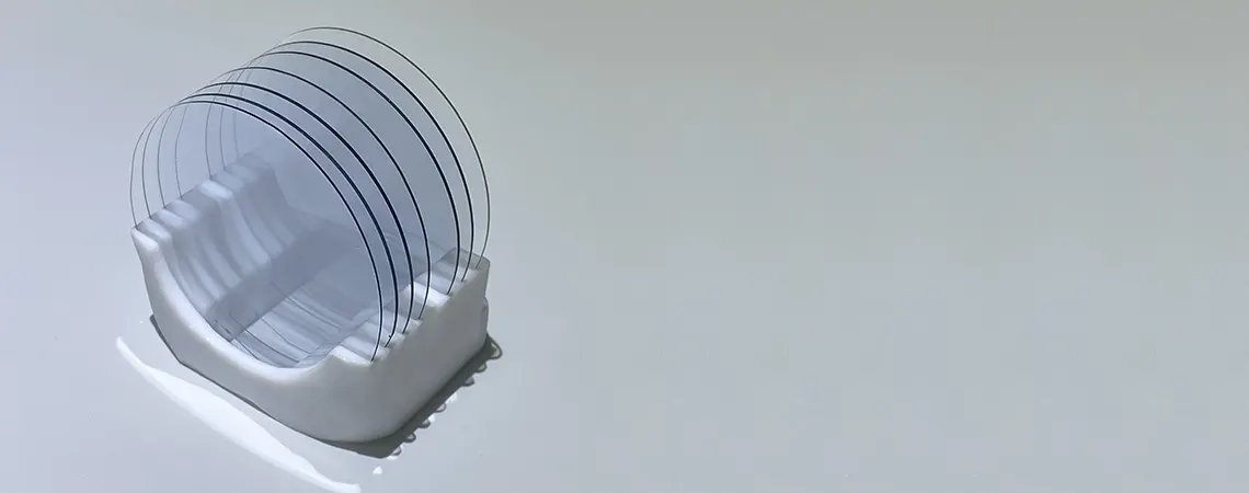
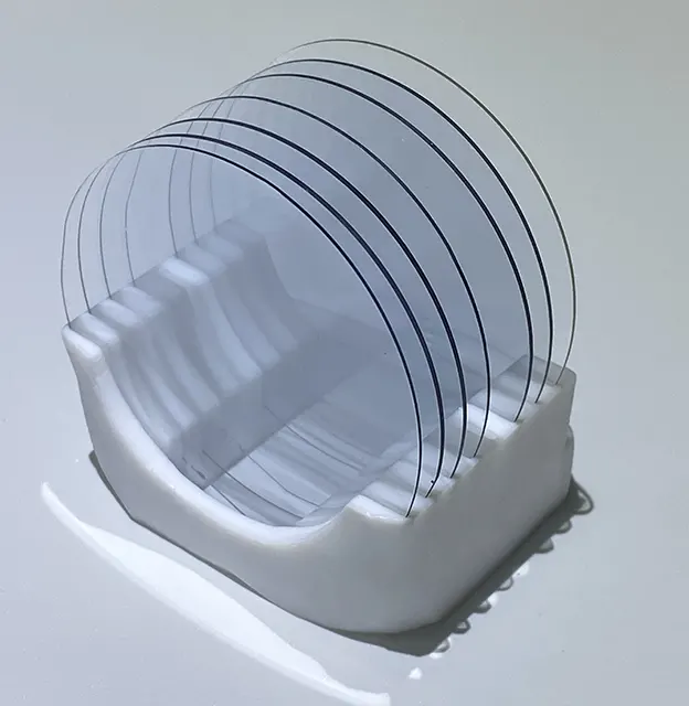
Ga₂O₃ Wafer
We Provide Ga₂O₃ Products.
- 10 × 10 Ga₂O₃ Square Substrate
- 1-inch Ga₂O₃ Wafer
- 2-inch Ga₂O₃ Wafer
- 4-inch Ga₂O₃ Wafer
- Ga₂O₃ Seed Crystal


Ga₂O₃ (gallium oxide) is used in wide range of fields as power electronic devices, taking advantage of its high breakdown voltage and low on-resistance characteristics. Specifically, they are used in electric vehicles, solar power inverters, and high-speed railway power transmission systems, and they have great potential in other fields as well.
Ga₂O₃ has band gap (forbidden band) width of 4.85 eV and excellent transmittance in visible light range, so it is expected to be used in fields such as solar blind ultraviolet exploration and radiation exploration.
Furthermore, by taking advantage of low mismatch characteristics of Ga₂O₃ single crystal and GaN (gallium nitride), it is being used as GaN growth substrate in production of high-performance high-frequency devices that are expected to be used in 5G communications.
10 × 10 Ga₂O₃ Square Substrate
| 10 × 10 Ga₂O₃ Square Substrate | |||
|---|---|---|---|
| Item | Specification | ||
| Crystal Orientation | (100) | ||
| Dopant | UID | Sn | Mg/Fe |
| Resistivity | 1016-1017 cm-3 | >1018 cm-3 | ≥1010 Ω·cm |
| FWHM (arcsec) | ≤150 | ||
| Dislocation Density | <1 × 105 cm-2 | ||
| Size | A-B | C-D | Thickness |
| 10 mm | 10.5 mm | 0.5(±0.02) mm | |
| Reference | Long side: [010] | ||
| Surface | Single-sided mirror/Double-sided mirror Ra < 0.5 nm Crystal surface deviation < ±1° |
||
 |
|||
1-inch & 2-inch Ga₂O₃ Wafer
| 1-inch & 2-inch Ga₂O₃ Wafer | |||
|---|---|---|---|
| Item | Specification | ||
| Crystal Orientation | (100) | ||
| Dopant | UID | Sn | Mg/Fe |
| Nd-Na/Resistivity | 1016-1017 cm-3 | >1018 cm-3 | ≥1010 Ω·cm |
| FWHM (arcsec) | ≤150 | ||
| Dislocation Density | <1 × 105 cm-2 | ||
| Size | Diameter | Thickness | |
| 25.4/50.8 ± 0.5 mm | 0.65 ± 0.02 mm | ||
| Reference | [010] | ||
| Surface | Single-sided mirror/Double-sided mirror Ra < 0.5 nm Crystal surface deviation < ±1° |
||
 |
|||
4-inch Ga₂O₃ Wafer
| 4-inch Ga₂O₃ Wafer | |||||||
|---|---|---|---|---|---|---|---|
| Item | Specification | ||||||
| Crystal Orientation | (100) | ||||||
| Doping | UID | Sn | Mg | ||||
| Nd-Na/Resistivity | 1016-1017 cm-3 | >1018 cm-3 | ≥1010 Ω・cm | ||||
| FWHM (arcsec) | ≤150 | ||||||
| Dislocation Density | <1 × 105 cm-2 | ||||||
| Size | Diameter | Thickness | |||||
| 100.0 ± 0.5 mm | 0.65 ± 0.02 mm | ||||||
| Reference | [010] | ||||||
| Surface | Single-sided mirror/Double-sided mirror Ra < 0.5 nm Crystal surface deviation < ±1° |
||||||
 |
|||||||
Ga₂O₃ Seed Crystal
| Ga₂O₃ Seed Crystal | |||
|---|---|---|---|
| Item | Specification | ||
| Crystal Orientation | Long-side Direction (100) | ||
| Doping | UID/Fe/Mg | ||
| FWHM (arcsec) | ≤150 | ||
| Dislocation Density | ≤2 × 104 cm-2 | ||
| Size | A-B | C-D | Length |
| 4-7 mm | 4-7 mm | 30-100 mm | |
| Surface | Cutting Surface Crystal surface deviation < ±1° |
||
 |
 |
||