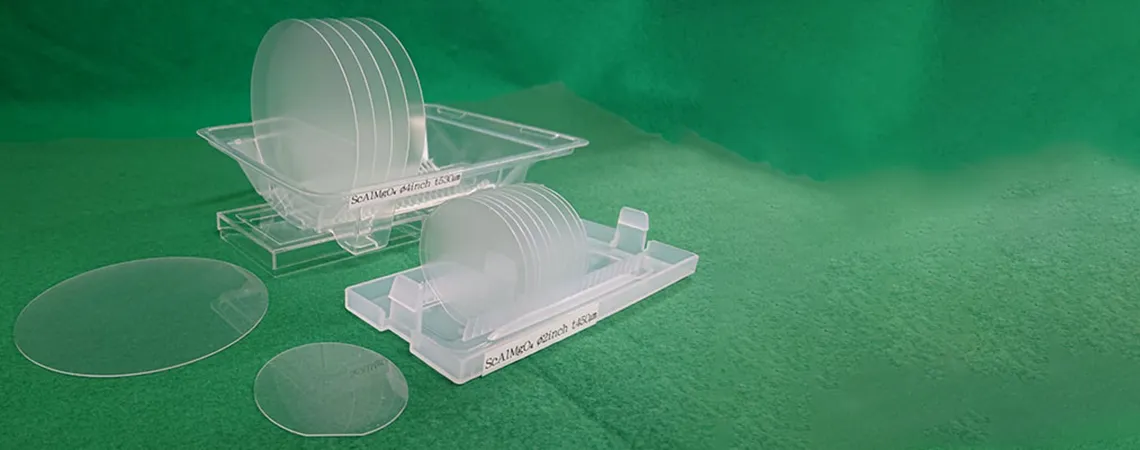
ScAlMgO4(SAM)ウェーハ
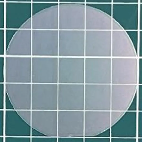
- 2~4インチSAMウェーハ
- 2~4インチSAMインゴット
- 10mm × 10mm MBE-GaN on SAM テンプレート
- 2インチMBE-GaN on SAM テンプレート
SAMウェーハは、LED、LD、FETなどのGaNデバイスの基板として有望です。
SAMウェーハ上に製造されるGaN自立基板は、自動車用途のGaNパワーデバイス用途に期待されています。
- 特徴
-
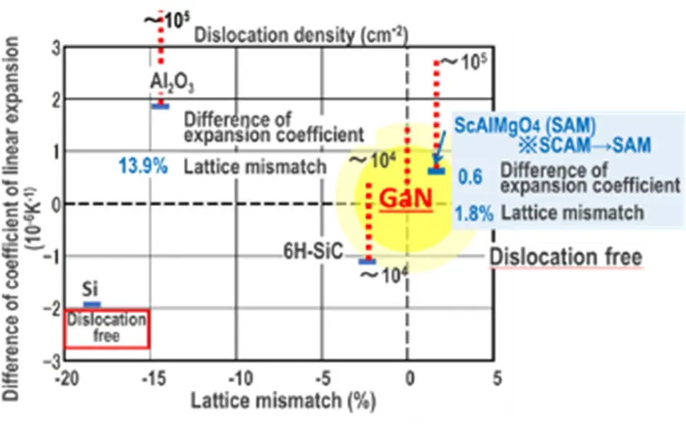
- GaNと格子不整合率小(不整合率 1.8%)
- InGaN と格子整合
- GaNと熱膨張率差小(膨張率差 0.6%)
- 劈開(へきかい)によってエピレディー基板を作製可能
- 無転位結晶を作製可能
- Siに匹敵する高品質結晶可能
ScAlMgO4 (SAM) Single Crystal Substrates
- Properties
-
- Bulk crystal development at AT&T Bell Laboratories in 1995
- Crystal structure YbFe2O4
- Space group 𝑅3 ̅𝑚
- Cleavage on C-plane
- Small lattice mismatch with GaN (about 1.3%)
- Small thermal expansion difference with GaN
- Crystals are grown by Czochralski method
| Sizes |
Wafer Orientation |
Orientation flat |
| 10 mm × 10 mm |
c |
ー |
| 2 inches |
c |
(10-10) |
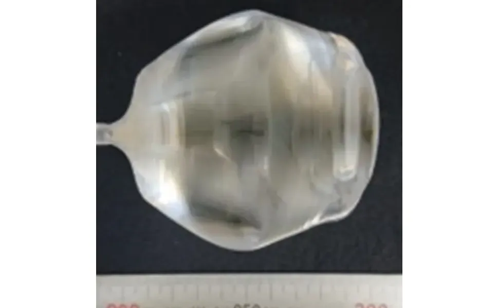 Ingot
Ingot
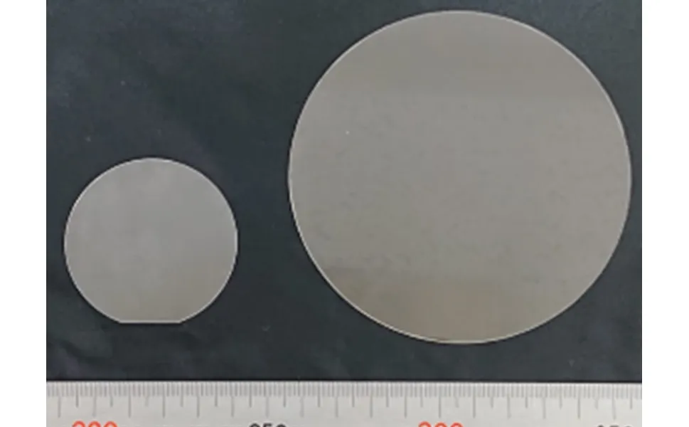 SAM Wafer
MBE-GaN on SAM Template
- Properties
-
- Direct GaN growth on SAM without buffer layer
- Low growth temperature
- Epitaxial growth of wurtzite GaN on SAM substrate with steep interface
- No obvious Mg diffusion in GaN thin film confirmed by SIMS
| Growth Methods |
Sizes |
Wafer orientation |
Orientation flat |
| MBE-GaN on SAM |
10 mm × 10 mm |
c |
ー |
| MBE-GaN on SAM |
2 inches |
c |
(10-10) |
 MBE-GaN on SAM Template
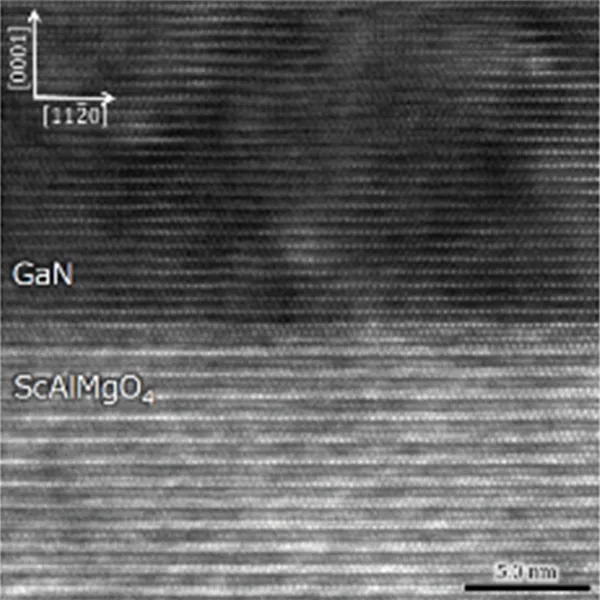 TEM of GaN / SAM interface
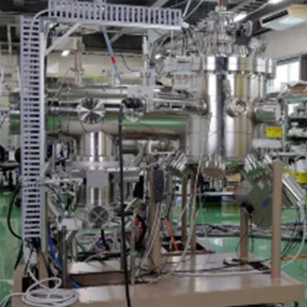 MBE Equipment