GaNウェーハ
GaNウェーハの製品を提供しております。
- 少量からのご注文
- パワーLSI、高輝度LED、レーザー用として注目
- 高品質(少ない結晶欠陥)
- 低価格(対他社比較)

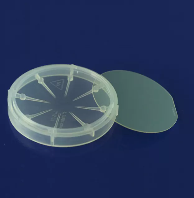
1~2インチGaN基板も扱っております。
GaN基板

| 項目 | 仕様 | ||
|---|---|---|---|
| 直径 | 51.0 mm ± 0.3 mm | 100.2 mm ± 0.3 mm | |
| 厚さ | 490 µm ± 30 µm | 540 µm ± 30 µm | |
| 面方位 | (0001) Ga-Face c-plane | ||
| TTV (5 mm edge exclusion) | ≤15 µm | ≤30 µm | |
| Warp (5 mm edge exclusion) | ≤20 µm | ≤80 µm | |
| Bow (5 mm edge exclusion) | -10 µm to +5 µm | -40 µm to +20 µm | |
| 電気特性 | タイプ | 抵抗率 | |
| N-type (Si) | ≤0.02 Ω·cm | ||
| UID | ≤0.2 Ω·cm | ||
| Semi-Insulating (Carbon) | >1E8 Ω·cm | ||
| グレード | Density (pits/cm2) | 2" (pits) | 4" (pits) |
| Production | ≤0.5 | ≤10 | ≤40 |
| Research | ≤1.5 | ≤30 | ≤120 |
| Dummy | ≤2.5 | ≤50 | ≤200 |
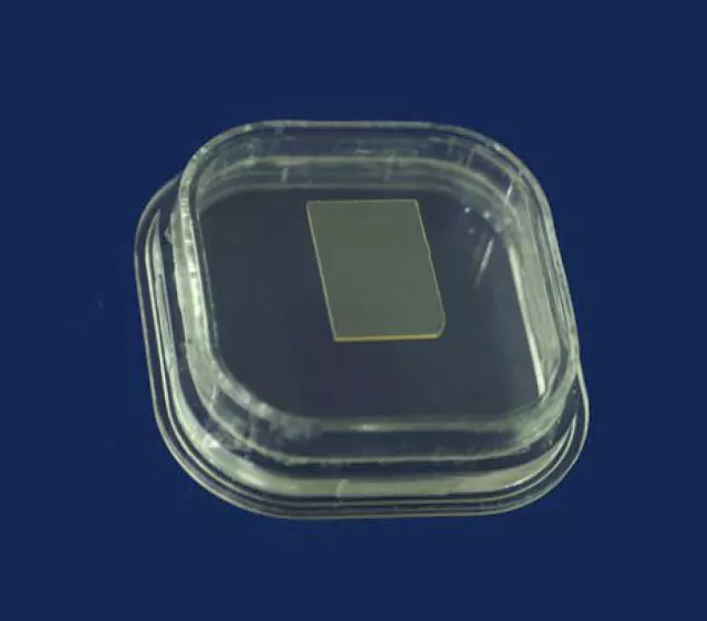
GaN基板(正方形)
| 項目 | 仕様 | ||
|---|---|---|---|
| サイズ | (10 ± 0.5) × (15 ± 0.5) mm2 Customized Size |
||
| 厚さ | 400 ± 25 µm | ||
| 面方位 | C-plane (0001) off-angle toward M-axis 0.35 ± 0.15° or 0.55 ± 0.15° |
||
| TTV | ≤10 µm | ||
| BOW | ≤10 μm | ||
| タイプ | UID | N-type (Si) | Semi-Insulating (Carbon) |
| Ga face surface roughness | <0.3 nm (10 × 10 μm) | ||
| N face surface roughness | Etched (0.5–1.5 µm); Polished (<0.3 nm) | ||
| 転位密度 | <1 × 106 cm2 | ||
| (002) FWHM | ≤70 arcsec | ||
| (102) FWHM | ≤70 arcsec | ||
| Macro defect density(hole) | <0.3 cm-2 | ||
| 有効面積 | >90% | ||
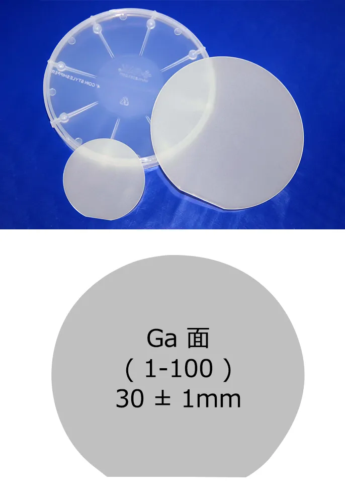
GaNテンプレート(φ2インチ)

| 項目 | 仕様 | |
|---|---|---|
| 直径 | φ50.8 mm ± 0.1 mm | |
| GaN膜厚 | 4 µm、10~25 µm | |
| 方位面 | C面(0001)面 ± 0.5° | |
| タイプ | UID | N-type (Si) |
| オリフラ方位。長さ | オリフラ方位(1~100)。オリフラ長さ 30 mm ± 1 mm | |
| 電気抵抗率(300 K) | <0.5 Ω·cm | <0.05 Ω·cm |
| 転位密度 | 5 × 108 cm2 | |
| 基板構造 | GaN/サファイアウェーハ(0001)面 | |
| 有効面積 | 90%以上 | |
| 表面仕上げ | Ga面:CMP仕上げ。N面:ファイングランディング(オプション:光学鏡面仕上げ) | |
GaNテンプレート(φ4インチ)
| 項目 | 仕様 |
|---|---|
| 直径 | φ100 mm ± 0.1 mm |
| GaN膜厚 | 4 µm、10~25 µm |
| 方位面 | C面(0001)面 ± 0.5° |
| 導電タイプ | N型(Undoped) |
| オリフラ方位。長さ | オリフラ方位(1~100)。オリフラ長さ 30 mm ± 1 mm |
| 電気抵抗率(300 K) | <0.5 Ω·cm |
| 転位密度 | 5 × 108 cm2 |
| 基板構造 | GaN/サファイアウェーハ(0001)面 |
| 有効面積 | 90%以上 |
| 表面仕上げ | Ga面:CMP仕上げ。N面:ファイングランディング(オプション:光学鏡面仕上げ) |
Power用GaN-on-Si エピウェーハ
| Items | Values/Scope |
|---|---|
| Wafer Diameter | 100mm, 150mm, 200mm, 300mm |
| Substrate | Si |
| Epi-layer Thickness | 2 ~ 7 μm |
| EWafer Bow | <30 μm, Typical |
| Surface Morphology | RMS < 0.5 nm (5 × 5 μm2) |
| Barrier | AlXGa1-XN (0 < x < 1) |
| Cap Layer | In-situ SiN or GaN (D-mode); p-GaN (E-mode) |
| 2DEG Density | >9E12/cm2 (20nm Al0.25GaN, 150mm) |
| Electron Mobility | >1800 cm2/Vs (20nm Al0.25GaN, 150mm) |
- 特徴
-
- 高電子移動度・高2DEG密度による優れたデバイス性能
- 低反り(Low Bow)による高いプロセス適合性
- 大口径(最大300 mm)対応による量産性向上
- D-mode / E-modeの両構造に対応可能
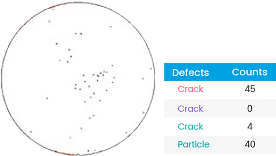
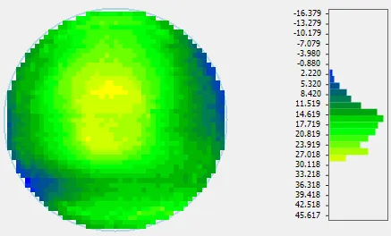
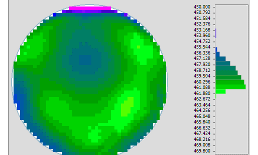
200mm GaN-on-Si Epiwafer
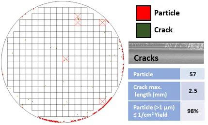
Defect Mapping
Vertical Breakdown Behavior
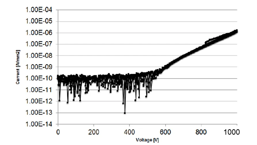
Sheet Resistance Mapping
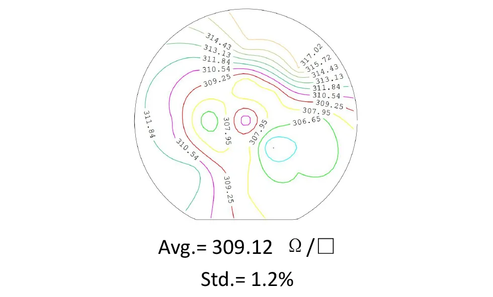
Wafer Bow Mapping
マイクロLED用GaN エピウェーハ
| Items | GaN-on-Si | GaN-on-Sapphire |
|---|---|---|
| 100mm, 150mm,200mm, 300mm | 50.8mm, 100mm, 150mm | |
| Epi-layer Thickness | <4 μm | <7 μm |
| Average Dominant/Peak Wavelength | 400–420 nm (near UV) | 270–280 nm (UVC) |
| 440–460 nm (Blue) | 440–460 nm (Blue) | |
| 510–530 nm (Green) | 510–530 nm (Green) | |
| - | 620–640 nm (Red) | |
| FWHM | <25nm for Blue/Near-UV <45nm for Green |
<15nm for UVC <25nm for Blue <40nm for Green |
| Wafer Bow | <50 μm | <180 μm |
- 特徴
-
- UVCから可視光(赤色)まで幅広い波長帯に対応
- 大口径(最大300 mm)のGaN-on-Siウェーハに対応
- 高品質エピタキシャル成長による優れた発光特性
- マイクロLED用途に適した高均一性・高精度エピ構造
200mm GaN-on-Si Epiwafer for Micro-LED
DDominant Wavelength
Avg: ~450 nm, Std<2 nm
Avg: ~450 nm, Std<2 nm
TDD: <1e9 cm-2
Defect Inspection
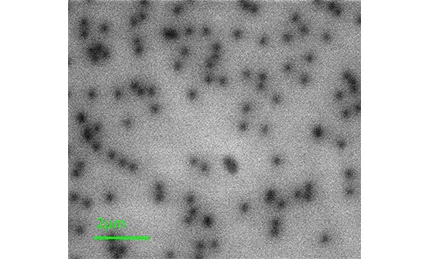
GaN-on-GaN エピウェーハ
- サイズ:2~4インチ
RF用 エピウェーハ
- GaN-on-Si:4~8インチ
- GaN-on-SiC:2~6インチ
- In-situ SiN/ Al(In)N/ GaNヘテロ構造
サイズ、エピ構造、膜厚等については、ご要望に応じてカスタマイズ対応が可能です。
詳細仕様については、ご要求に応じて最適化可能です。