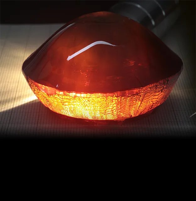
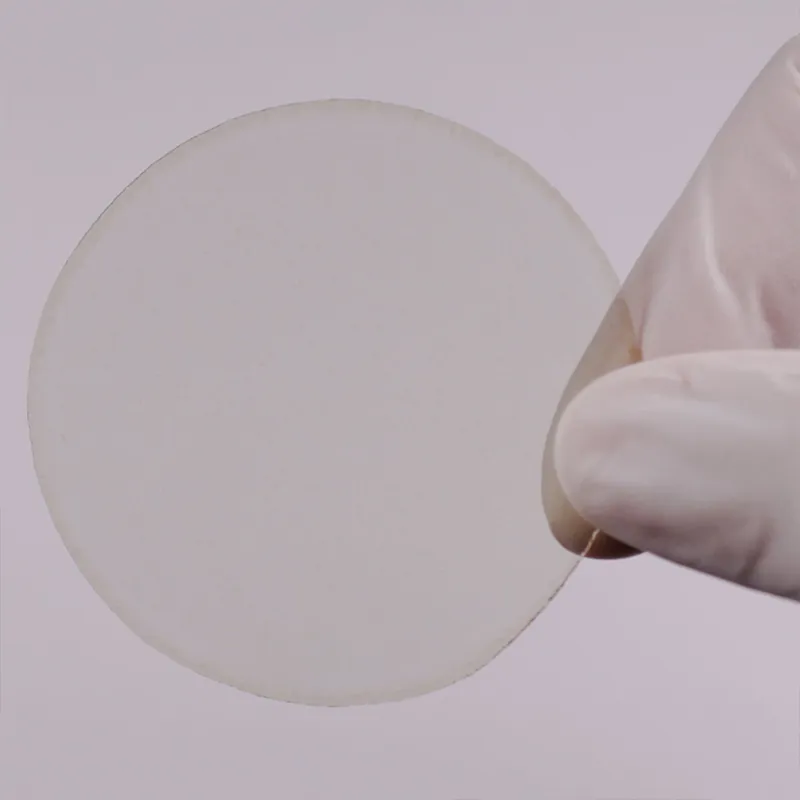
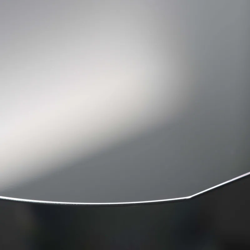
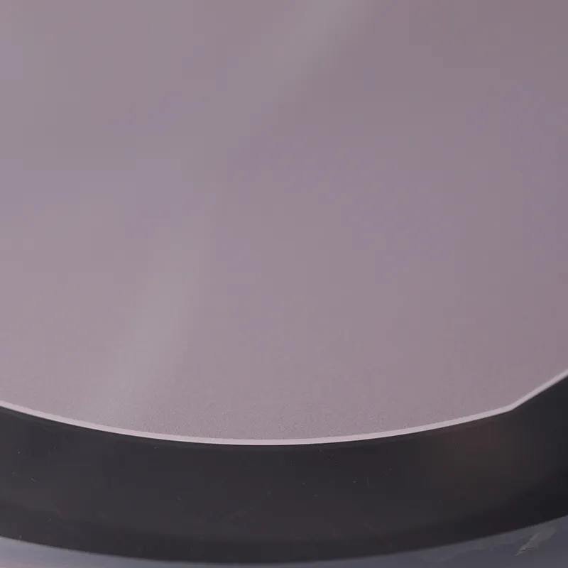
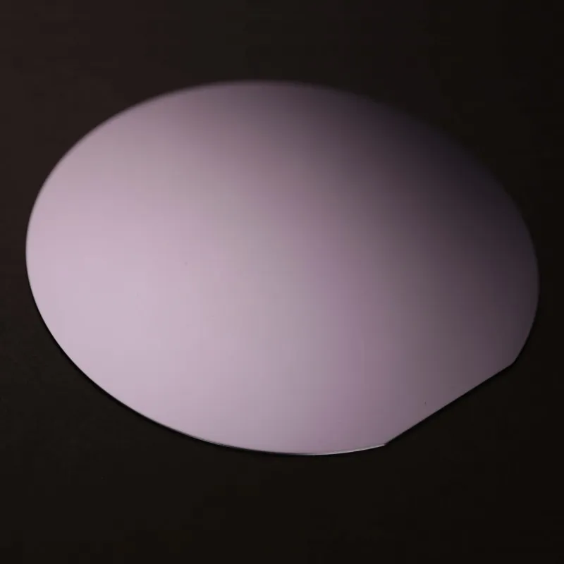
窒化アルミニウム(AlN)
窒化アルミニウム(AlN)単結晶基板は、高い熱伝導率、優れた電気絶縁性、低誘電損失、耐熱性を備えた次世代の電子材料です。特に、パワーエレクトロニクス、高周波デバイス、UV-LED、深紫外(DUV)光源、半導体パッケージなどの用途に適しています。
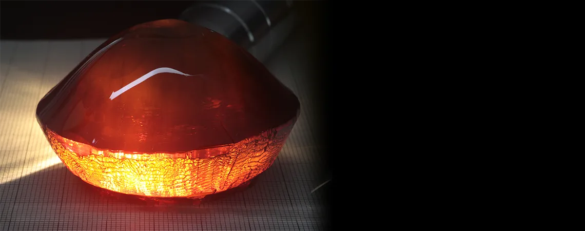
窒化アルミニウム(AlN)単結晶の製品をご提供しております。
ご希望の仕様についても対応可能ですので、お気軽にお問い合わせください。
窒化アルミニウム(AlN)単結晶基板
| Diameter (mm) | 10-50.8 mm or 10 × 10 mm or 10-20 mm or 5 mm-50.8 mm | ||
|---|---|---|---|
| Thickness (µm) | 400 ± 50 | ||
| Crystal Type | 2H | ||
| Orientation | {0001} ± 0.5° | ||
| Surface Finish | Al face: CMP (double side polishing is customizable) | ||
| Roughness | Al face: ≤0.5 nm N face (backside): ≤1.2 μm |
||
| Shape | Round / Rectangle / Quadrangle | ||
| Grade | S (Super) | P (Production) | R (Research) |
| FWHM-HRXRD@(0002) (arcsec) | ≤150 | ≤300 | ≤500 |
| FWHM-HRXRD@(10-12) (arcsec) | ≤100 | ≤200 | ≤400 |
| Absorption Coefficient@265nm (cm-1) | ≤50 | ≤70 | ≤100 |
| Edge Exclusion (mm) | 1 | 1 | 1 |
| Scratches | None | None | None |
| Edge Chips | None | None | ≤3total cumulative length≤1.0 mm |
| Usable Area | ≥90% | ||
| Primary Flat Orientation | {10-10} ± 5.0° | ||
| Secondary Flat Orientation | 90°±5 CW from Primary Flat, as viewed from Al face 90°±5 CCW from Primary Flat, as viewed from N face |
||
| TTV (µm) | ≤30 | ||
| Bow (µm) | ≤30 | ||
| Wrap (µm) | ≤30 | ||
| Cracks | None, by naked eye, high intensity light | ||
| Surface Contamination | None, by naked eye, diffuse light | ||
| Laser Marking | N face, parallel to primary flat | ||
| Packaging | Single wafer cups | ||
| Element | C | O | Si | B | Na | W | P | S | Ti | Fe |
|---|---|---|---|---|---|---|---|---|---|---|
| PPMW | 81 | 110 | 9.7 | 0.92 | 0.23 | <0.1 | <0.1 | <0.5 | 0.46 | <0.5 |
| Properties | Reference |
|---|---|
| Crystal Structure | Wurtzite |
| Lattice Constant (Å) | a=3.112, c=4.982 |
| Conduction Band Type | Direct Bandgap |
| Density (g/cm3) | 3.23 |
| Surface Microhardness (Knoop test) | 800 |
| Melting Point (℃) | 2750 (10-100 bar in N2) |
| Thermal Conductivity (W/m·K) | 320 |
| Band Gap Energy (eV) | 6.28 |
| Electron Mobility (V·s/cm2) | 1100 |
| Electric Breakdown Field (MV/cm) | 11.7 |
| Acoustic Wave Velocity (m/s) | 11300 |
Sapphire on AlScNテンプレート
| Diameter (inch) | 2 | 4 | 6 |
|---|---|---|---|
| Substrate | C-plane of sapphire | ||
| Substrate Thickness (µm) | 430 ± 15 | 650 ± 20 | 1300 ± 20 |
| Sc Concentration (at%) | 40 ± 5 | ||
| AlScN Film thickness (nm) | 800 | ||
| Orientation | C-axis [0001] +/- 0.2° | ||
| Usable Area | ≥95% | ||
| Cracks | None | ||
| FWHM-HRXRD@(0002) (arcsec) | ≤120 | ||
| Surface Roughness@[5 × 5µm] (nm) | ≤10 | ||
| TTV (µm) | ≤10 | ≤20 | ≤20 |
| Bow (µm) | ≤20 | ≤40 | ≤60 |
| Warp (µm) | ≤20 | ≤40 | ≤60 |
| Packaging | Single/Multi Wafer Cups | ||
Si on AlScNテンプレート
| Diameter (inch) | 4 | 6 | 8 |
|---|---|---|---|
| Substrate | C-plane of Si single crystal wafer | ||
| Substrate Thickness (µm) | 525 ± 20 | 625 ± 15 | 725 ± 15 |
| Sc Concentration(at%) | 40 ± 5 | ||
| Conductivity Type | N/P | ||
| AlScN Film thickness (nm) | 800 | ||
| Orientation | C-axis [0001] +/- 0.2° | ||
| Usable Area | ≥95% | ||
| Cracks | None | ||
| FWHM-HRXRD@(0002) (arcsec) | ≤2° | ||
| Surface Roughness@[5 × 5µm] (nm) | ≤5 | ||
| TTV (µm) | ≤10 | ≤5 | ≤40 |
| Bow (µm) | ≤25 | ≤40 | ≤40 |
| Warp (µm) | ≤25 | ≤40 | ≤40 |
| Packaging | Single/Multi Wafer Cups | ||
Sapphire on AlNテンプレート
| Substrate | C-plane of sapphire | ||
|---|---|---|---|
| AlN Structure | Wurtzite | ||
| Diameter (inch) | 2 | 4 | 6 |
| Substrate Thickness (µm) | 430 ± 15 | 650 ± 20 | 1300 ± 20 |
| AlN Film thickness (nm) | 200/400/600/800/1000 (Technical specs may vary with AlN film thickness, hereby taking 200nm as an example) |
||
| Orientation | C-axis [0001] +/- 0.2° | ||
| Usable Area | ≥95% | ||
| Cracks | None | ||
| Back Surface Finish (µm) | RMS<1.2 | ||
| FWHM-HRXRD@(0002) (arcsec) | <100 | ||
| FWHM-HRXRD@(10-12) (arcsec) | <350 | ||
| Surface Roughness@[5 × 5µm] (nm) | Ra≤2 | ||
| TTV (µm) | ≤10 | ≤20 | ≤20 |
| Bow (µm) | ≤20 | ≤40 | ≤60 |
| Warp (µm) | ≤20 | ≤40 | ≤60 |
| Packaging | Single/Multi Wafer Cups | ||
Si on AlNテンプレート
| Substrate | C-plane of Si single crystal wafer | ||
|---|---|---|---|
| Conductivity Type | N/P | ||
| Resistivity (Ω) | >5000 | ||
| AlN Structure | Wurtzite | ||
| Diameter (inch) | 4 | 6 | 8 |
| Substrate Thickness (µm) | 525 ± 20 | 625 ± 15 | 725 ± 15 |
| AlN Film Thickness (nm) | 200/400/600/800/1000 (Technical specs may vary with AlN film thickness, hereby taking 500nm as an example) |
||
| Orientation | C-axis [0001] +/- 0.2° | ||
| Usable Area | ≥95% | ||
| Cracks | None | ||
| FWHM-2θXRD@ (0002) | ≤0.2° | ||
| FWHM-HRXRD@ (0002) | ≤1.55° | ||
| Surface Roughness [5 × 5µm] (nm) | ≤2.0 | ||
| TTV (µm) | ≤10 | ≤5 | ≤4 |
| Bow (µm) | ≤25 | ≤40 | ≤40 |
| Warp (µm) | ≤25 | ≤40 | ≤40 |
| Packaging | Single/Multi Wafer Cups | ||