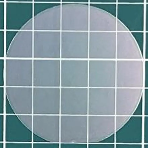
ScAlMgO4 (SAM) Wafer
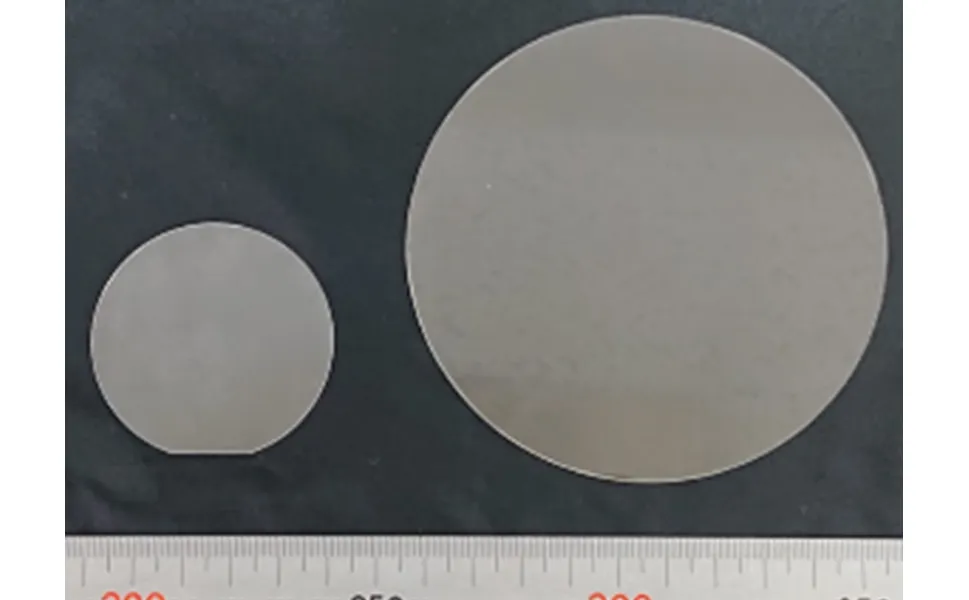
2-4 inch SAM Wafer
2-4 inch SAM Ingot
10 mm × 10 mm MBE-GaN on SAM Template
2-inch MBE-GaN on SAM Template
SAM wafers are promising as substrates for GaN devices such as LEDs, LDs, and FETs.
GaN freestanding substrates manufactured on SAM wafers are expected to be used for GaN power devices in automotive applications.
- Features
-
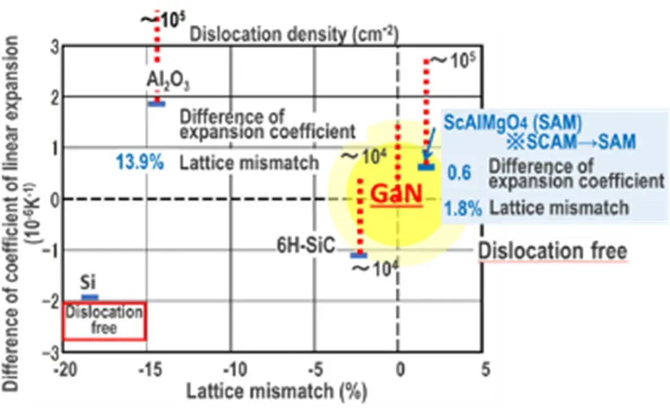
- Small lattice mismatch with GaN (Mismatch rate 1.8%)
- Lattice-matched with InGaN
- Small thermal expansion difference with GaN (Expansion difference 0.6%)
- Epitaxial substrates can be created by cleavage.
- Dislocation-free crystals can be created.
- High-quality crystals comparable to Si can be produced.
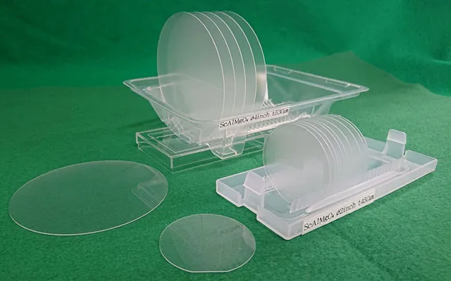
ScAlMgO4 (SAM) Single Crystal Substrates
- Properties
-
- Bulk crystal development at AT&T Bell Laboratories in 1995
- Crystal structure YbFe2O4
- Space group 𝑅3 ̅𝑚
- Cleavage on C-plane
- Small lattice mismatch with GaN (about 1.3%)
- Small thermal expansion difference with GaN
- Crystals are grown by Czochralski method
| Sizes | Wafer Orientation | Orientation flat |
|---|---|---|
| 10 mm × 10 mm | c | ー |
| 2 inches | c | (10-10) |
MBE-GaN on SAM Template
- Properties
-
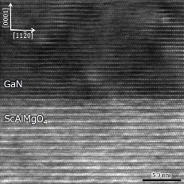
- Direct GaN growth on SAM without buffer layer
- Low growth temperature
- Epitaxial growth of wurtzite GaN on SAM substrate with steep interface
- No obvious Mg diffusion in GaN thin film confirmed by SIMS
| Growth Methods | Sizes | Wafer orientation | Orientation flat |
|---|---|---|---|
| MBE-GaN on SAM | 10 mm × 10 mm | c | ー |
| MBE-GaN on SAM | 2 inches | c | (10-10) |
