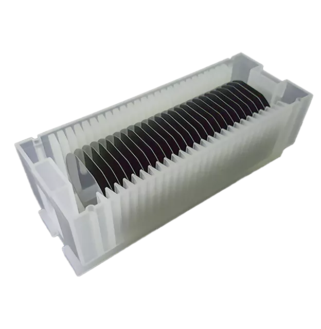
Germanium Wafer
Germanium (Ge) is a semiconductor with a smaller band gap than silicon (about 0.7 eV). It can have three structures that change with temperature and pressure, shifting from a stable diamond to a cubic structure under high pressure.


- Applications and Fields
- Ge wafers are important semiconductor substrate materials. These high-quality substrates are mainly used in Concentrated Photovoltaic (CPV), space solar cell panels, and high-brightness light-emitting diode applications.
| Item | Unit | Specifications | |
|---|---|---|---|
| Crystal Growth Method | CZ/VGF | ||
| Type | N-type | P-type | |
| Dopant | As, Sb | Ga | |
| Diameter | inch | 2-6 | |
| Surface Orientation | (100) ± 0.5° | ||
| Off Orientation | US, EJ | ||
| Thickness | μm | (175-500) ± 25 | |
| Resistivity | Ω·cm | 0.005-30 | 0.005-0.04 |
| Dislocation Density (EPD) | cm2 | - | 0 |
| TTV | μm | ≤15 | ≤15 |
| Warp | μm | ≤25 | ≤25 |
| Back Surface Roughness (Ra) | μm | <0.1 | <0.1 |
| Surface Finish | Front Surface/Back Surface | Mirror/Etching, Etching/Etching | |
| Packaging Method | Coin Roll/Cassette Case | ||