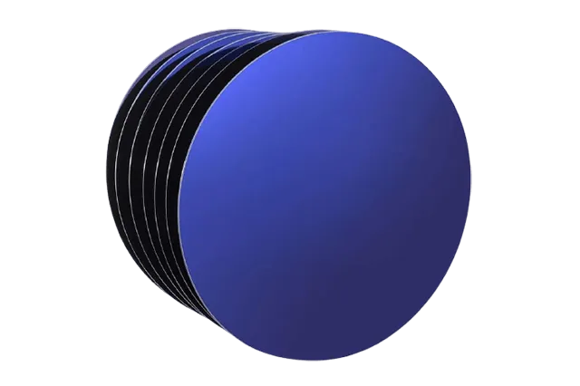
SOI Wafer
We offer high-quality SOI wafers ranging from 4 to 12 inches.
SOI wafers are composed of three layers: the top layer (device layer), the middle oxide layer (insulating SiO2 layer), and the bottom substrate (handle silicon). They are manufactured using SIMOX method and wafer bonding technology. This allows for a thinner and more accurate device layer, uniform thickness, and lower defect density.
SOI wafers provide an excellent solution for high-speed and low-power devices, and are widely recognized as a new solution for high-voltage and RF devices.
Our company realizes the processing and supply of multi-specification and high-quality substrates ranging from 4 to 12 inches.
We can accommodate active layer thicknesses of 1μm and above, and our products are used in a variety of scenarios, including various device development and research.
We can propose solutions tailored to your needs, such as embedded oxide films and resistance values.
SOI Wafer Product Specification Compatibility Table
| Size | inch | 4 | 5 | 6 | 8 | 12 |
|---|---|---|---|---|---|---|
| Active Layer | Unit | Specification | ||||
| Manufacturing Method | - | CZ / FZ | ||||
| Type & Conductivity Type | - | P / N / Non-doped | ||||
| Crystal Orientation | - | <100> / <111> / <110> | ||||
| Dopant | - | B、P、As、Sb | ||||
| Thickness | μm | ≧1.0 | ||||
| *Resistivity | Ω・㎝ | 0.001 ~ 10000 | ||||
| *Buried Oxide Film | μm | 0.05 ~ 10 | ||||
| Support Substrate | Specification | |||||
| Manufacturing Method | - | CZ / FZ | ||||
| Type & Conductivity Type | - | P / N / ノンドープ | ||||
| Crystal Orientation | - | <100> / <111> / <110> | ||||
| Dopant | - | B、P、As、Sb | ||||
| *Thickness | μm | JEITA・SEMI standard / 200 ~ 1500 | ||||
| *Resistivity | Ω・㎝ | 0.001 ~ 10000 | ||||
| Remarks | *Please inquire separately for detailed specifications. | |||||