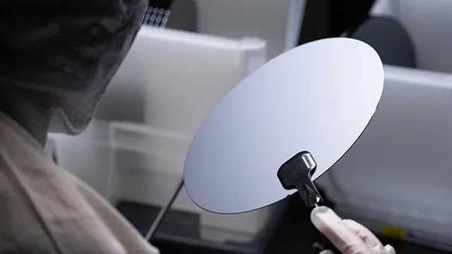
Silicon Wafer
"A wafer generally refers to something that is thin and plate-shaped. In the context of semiconductors, it refers to thin plate-shaped single crystals of Si or similar materials, which serve as the substrate for semiconductor devices. These are referred to as Si wafers, etc. Currently, the mainstream size for Si wafers is 200mm (8 inches), and the use of 300mm (12 inch) wafers has also begun.
We provide silicon wafers used as semiconductor substrates ranging in size from 2 inches to 12 inches, tailored to the usage needs and requests of our customers.
We provide wafers suitable for the usage purposes and planning of many manufacturers, universities, and research institutes, using a variety of products from major manufacturers.
We will fulfill your needs by providing wafers of assured quality.
| Items | Unit | Specification | ||||||
|---|---|---|---|---|---|---|---|---|
| Size | inch | 2 | 3 | 4 | 5 | 6 | 8 | 12 |
| Thickness | μm | 280±25 | 380±25 | 525±25 | 625±25 | 625±25 | 725±25 | 775±25 |
| Manufacture | - | CZ or FZ | ||||||
| Crystal Orientation | - | <100> or <111>or no preference | ||||||
| Type | - | P/N/No preference | ||||||
| Resistance Value | Ω・cm | 0.01~1,000Ω・cm | ||||||
| Surface Finish | - | Double-sided/Single-sided Mirror | ||||||
| Back Surface Finish | - | Double-sided/Single-sided Mirror | ||||||
| Packing Form | - | Laminate/Coin Roll | ||||||
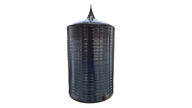
Silicon Ingot
- Product Description
- We produce monocrystalline ingots, which serve as the material for silicon wafers, using a manufacturing method known as the Czochralski process (CZ method).
- Primarily used in the etching process, a part of the device manufacturing process, it is an extremely important consumable material. We can provide silicon ingot products of various sizes and resistivities according to customer requirements.
| Diameter in mm | Type | Crystal Orientation | Purity | Resistivity (Ω.cm) | Length |
|---|---|---|---|---|---|
| φ200-φ550 | P | <100>/<111> | 10~11N | ≤0.01 | Custom-made |
| 1-4 | |||||
| 60-90 | |||||
| Custom-made |