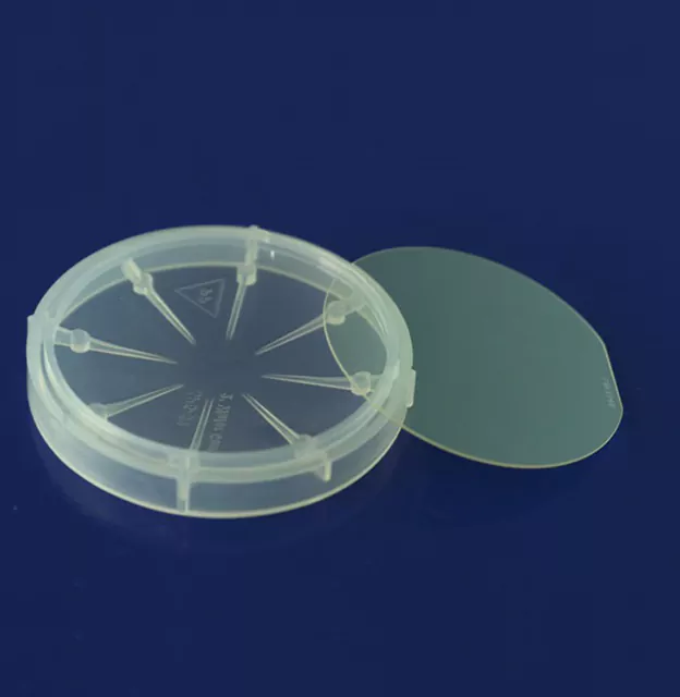
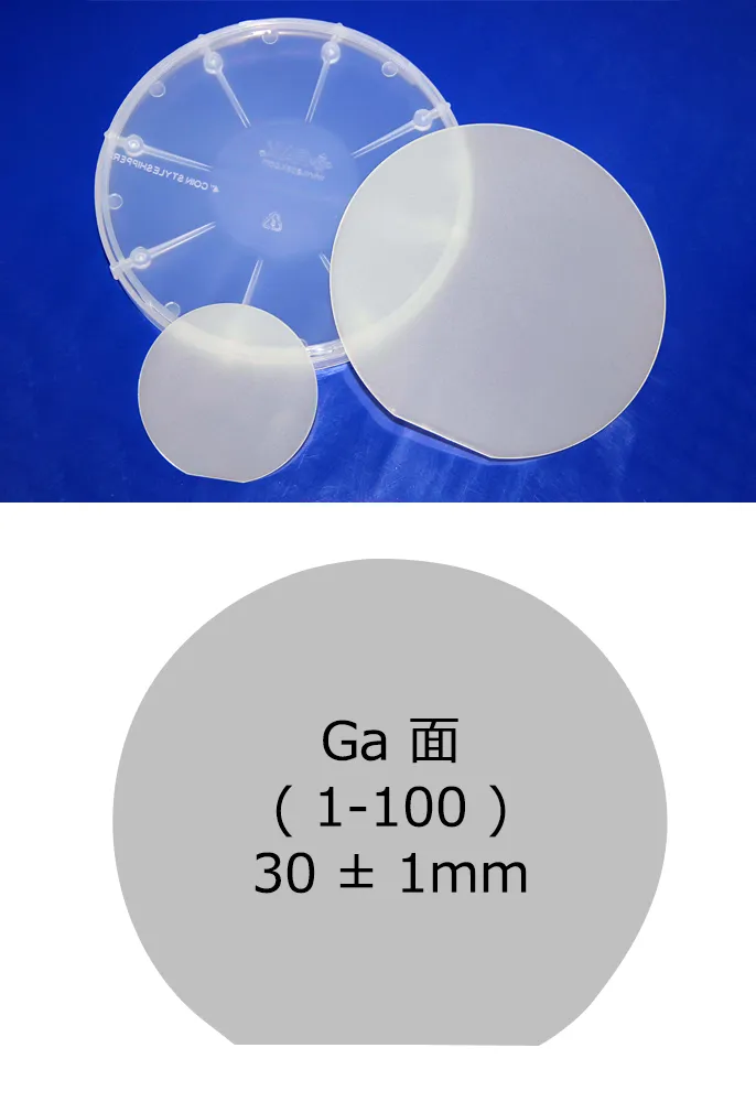
GaN Wafer
We provide GaN Wafer products.
- Accepting small quantity orders.
- Noteworthy for use in Power LSI, high-brightness LEDs, and lasers.
- High quality (few crystal defects).
- Competitively priced (compared to other companies).

Highlighted for use in Power LSI, high-brightness LEDs, and high-performance lasers.
GaN Substrate

| Items | Specifications | ||
|---|---|---|---|
| Diameter | 51.0 mm ± 0.3 mm | 100.2 mm ± 0.3 mm | |
| Thickness | 490 um ± 30 um | 540 um ± 30 um | |
| Surface Orientation | (0001) Ga-face c-plane | ||
| TTV (5 mm edge exclusion) | ≤ 15 um | ≤ 30 um | |
| Warp (5 mm edge exclusion) | ≤ 20 um | ≤ 80 um | |
| Bow (5 mm edge exclusion) | -10 um to + 5 um | -40 um to +20 um | |
| Electrical characteristics | Type | Resistivity | |
| N-type (Silicon) | ≤ 0.02 ohm-cm | ||
| UID | ≤ 0.2 ohm-cm | ||
| Semi-Insulating (Carbon) | > 1E8 ohm-cm | ||
| Grade | Density (pits/cm2) | 2" (pits) | 4" (pits) |
| Production | ≤ 0.5 | ≤ 10 | ≤ 40 |
| Research | ≤ 1.5 | ≤ 30 | ≤ 120 |
| Dummy | ≤ 2.5 | ≤ 50 | ≤ 200 |
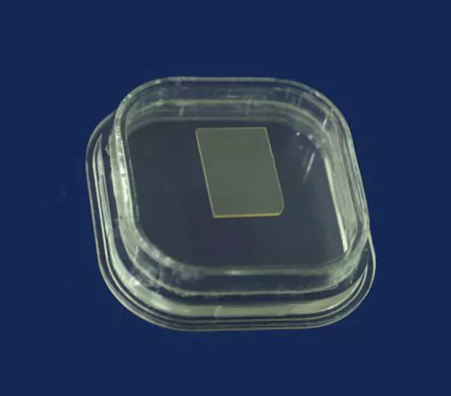
GaN Substrate (Square)
| Item | Specification | ||
|---|---|---|---|
| Size | (10±0.5)×(15±0.5)mm² Customized Size |
||
| Thickness | 400±25 μm | ||
| Surface Orientation | Cplane (0001)off angle toward M-axis 0.35±0.15°or 0.55±0.15° |
||
| TTV | ≤ 10 μm | ||
| BOW | ≤ 10 μm | ||
| Conductive Type | N-type (Un-doped) |
N-type (Silicon-doped) |
Semi-Insulating (Carbon-doped) |
| Ga face surface roughness | < 0.3 nm(10×10μm) | ||
| N face surface roughness | Etched(0.5~1.5μm);Polished(<0.3nm) | ||
| Dislocation Density | < 1×106cm-2 | ||
| (002)FWHM | ≤ 70 arcsec | ||
| (102)FWHM | ≤ 70 arcsec | ||
| Macro defect density(hole) | < 0.3 cm-2 | ||
| Effective Area | > 90% | ||
GaN Template (φ2 Inch)

| Item | Specification | |
|---|---|---|
| Diameter | φ50.8mm ± 0.1mm | |
| GaN Film Thickness | 4um. 10-25um | |
| Orientation Plane | C-plane (0001) face ± 0.5° | |
| Conductivity Type | N-type (Undoped) | N-type (Si-doped) |
| Orientation. Length | Orientation (1-100). Orientation length 16 ± 1mm | |
| Electrical resistivity (300K) | < 0.5Ω·cm | < 0.05Ω・cm |
| Transition defect density | 5 × 10⁸ pieces/cm2 or less | |
| Substrate Structure | GaN / Sapphire wafer (0001) surface | |
| Effective Area | 90% or more | |
| Surface Finish | Ga face: CMP finish. N face: fine grinding (option: optical mirror finish) | |
| Packing Method | Packed in a clean room with nitrogen. Each piece is individually packed, or in a 25-piece cassette. | |
GaN Template (φ4 inches)
| Item | Specifications |
|---|---|
| Diameter | φ100mm ± 0.1mm |
| GaN Film Thickness | 4um. 10~25um |
| Orientation Plane | C-plane (0001) ± 0.5° |
| Conductivity Type | N-type (Undoped) |
| Orientation Flat. Length | Orientation Flat (1-100). Flat length 30 ± 1mm |
| Electrical Resistivity (300K) | < 0.5Ω・cm |
| Transition Defect Density | 5 × 10⁸ pieces/cm2 or less |
| Substrate Structure | GaN / Sapphire Wafer (0001) Surface |
| Effective Area | 90% or more |
| Surface Finish | Ga surface: CMP finish. N surface: Fine grinding (Option: Optical mirror finish) |
| Packing Method | Packed in a clean room with nitrogen. Each piece is packaged individually, or in a 25-piece cassette. |
2inch GaN-on-Sapphire Blue/Green LED Wafer

| Substrate | Type | Flat Sapphire | |
|---|---|---|---|
| Polish | Single side polished(SSP)/Double side polished(DSP) | ||
| Dimension | 50.8±0.2mm | ||
| Orientation | Cplane(0001)off angletoward M-axis0.2±0.1° | ||
| Thickness | 430±25mm | ||
| Epilayer | Structure | 0.2μm pGaN/0.5μm MQWs/2.5μm nGaN/2.0μm uGaN | |
| Thickness | 5.5±0.5μm | ||
| Roughness(Ra) | <0.5nm | ||
| Dislocation density | <5×108cm2 | ||
| Wavelength | Blue LED | Green LED | |
| 465±10nm | 525±10nm | ||
| Wavelength FWHMs | <25nm | <40nm | |
| Chip Performance | Cut-in voltage@1μA | 2.3-2.5V | 2.2-2.4V |
| Useable Area | >90%(edge and macro defects exclusion) | ||
| Package | Packaged in a cleanroom in a single wafer container | ||
4inch GaN-on-Sapphire Blue/Green LED Wafer

| Substrate | Type | Flat Sapphire | ||
|---|---|---|---|---|
| Polish | Single side polished(SSP)/Double side polished(DSP) | |||
| Dimension | 100±0.2mm | |||
| Orientation | Cplane(0001)off angletoward M-axis0.2±0.1° | |||
| Thickness | 650±25μm | |||
| Epilayer | Structure | 0.2μm pGaN/0.5μm MQWs/2.5μm nGaN/2.0μm uGaN | ||
| Thickness | 5.5±0.5μm | |||
| Roughness(Ra) | <0.5nm | |||
| Dislocation density | <5×108cm2 | |||
| Wavelength | Blue LED | Green LED | Red LED | |
| 465±10nm | 525±10nm | 630±10nm | ||
| Wavelength FWHMs | <25nm | <40nm | ||
| Chip Performance | Cut-in voltage@1μA | 2.3-2.5V | 2.2-2.4V | |
| Useable Area | >90%(edge and macro defects exclusion) | |||
| Package | Packaged in a cleanroom in a single wafer container | |||
6inch GaN-on-Sapphire Blue/Green/Red LED Wafer

| Substrate | Type | Flat Sapphire | ||
|---|---|---|---|---|
| Polish | Single side polished(SSP)/Double side polished(DSP) | |||
| Dimension | 150±0.2mm | |||
| Orientation | Cplane(0001)off angletoward M-axis0.2±0.1° | |||
| Thickness | 1300±25μm | |||
| Epilayer | Structure | 0.2μm pGaN/0.5μm MQWs/2.5μm nGaN/2.0μm uGaN | ||
| Thickness | 6.9±0.5μm | |||
| Roughness(Ra) | <0.5nm | |||
| Dislocation density | <5×108cm2 | |||
| Wavelength | Blue LED | Green LED | Red LED | |
| 475±3nm | 521±5nm | 630±8nm | ||
| Wavelength FWHMs | <25nm | <40nm | ||
| Chip Performance | Cut-in voltage@1μA | 2.3-2.5V | 2.2-2.4V | |
| Useable Area | >90%(edge and macro defects exclusion) | |||
| Package | Packaged in a cleanroom in a single wafer container | |||