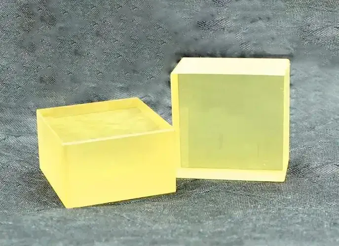
ZnO Acidified Zinc Oxide
Piezoelectric sensors, SAW devices, LEDs, scintillators, ultraviolet sensors, transistors, and other applications make zinc oxide a highly valuable material for next-generation semiconductors.

ZnO·C Plate Substrate Standard Specifications (+C Region)
| Surface Orientation | 0001 Plate (C-Plane, +C Region) |
|---|---|
| Dimensions: | 10mm Substrate: 10.0 mm ± 0.2 × 10.0 mm ± 0.2, t = 0.5 mm ± 0.2 20mm Substrate: 20.0 mm ± 0.2 × 10.0 mm ± 0.2, t = 0.5 mm ± 0.2 |
| Angle | 0.0° ± 0.5° for each axis direction |
| Surface Finish | Double-sided Polished Finish |
| Surface Roughness | RMS < 1.0nm |
| Impurity Concentration | Fe: 0.30 wt%, Li: 0.61 wt%, Al: <0.20 wt%, Ca: 0.11 wt%, Mg: 0.38 wt%, K: 0.82 wt%, Cr: <0.20 wt% Ni: 0.65 wt%, Na: 0.09 wt%, Ga: 0.16 wt%, Mo: <0.01 wt%, V: <0.01 wt%, Cu: 0.03 wt% |
| Mobility | 100~200 cm2/(V·s) |
| Carrier Concentration | 1E+15~16cm3 |
| Resistivity | 0.1~10kΩcm |
| Crystallinity | FWHM (0002) < 25 arc seconds |
Standard Size
| Product | Size |
|---|---|
| Wafer | 10 × 10 × 0.5 mm 20 × 20 × 0.5 mm |
| Block | 10 × 10 × 5~7 mm |