Quartz Substrates for Photomasks
Application:
Substrates such as TGV, DOE, PLC, AWG, etc.
Features:
Extremely low metal impurity content
High refractive index uniformity
Bubble-free
High surface gloss and smoothness
OH content <50 ppm
High refractive index uniformity
Bubble-free
High surface gloss and smoothness
OH content <50 ppm
Optical Properties
| Model | OH (ppm) | Stress Birefringence (nm/cm) | Streak Grade | Transmittance | Internal Transmittance | Recommended Wavelength Range |
|---|---|---|---|---|---|---|
| TSM-6025I | <250 | <10 | 1D | >90.2%@365nm | >99.8%@193/248/365nm | Ultraviolet Region & Visible Region |
| TSM-6025K | <250 | <2 | 1D | >90.2%@248nm | >99.8%@193/248/365nm | KrF |
| TSM-6025A | <50 | <1 | 3D | >90.2%@193nm | >99.8%@193/248/365nm | ArF |
Processing and Inspection Capability
Processing and inspection of quartz substrates for semiconductor mask plates are supported.
- Wire saw processing supported
- CNC precision processing (high-precision cutting supported)
- Double-sided grinding and double-sided polishing supported
- Ultrasonic cleaning and deep cleaning supported
- Defect inspection supported
Flatness measurement (using AFM) supported
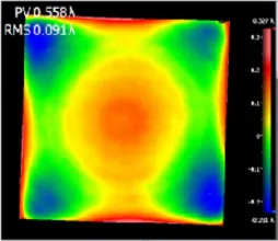
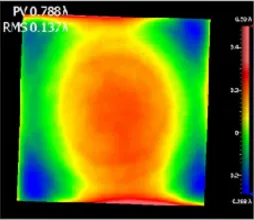
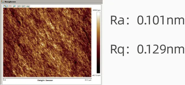
Surface roughness measurement (measurement range: 10 μm × 10 μm)
| Grade | I-line | KrF | ArF |
|---|---|---|---|
| Front (um) | ≤2 | ≤1 | ≤0.5 |
| Back (um) | ≤3 | ≤2 | ≤1 |
| TTV (um) | ≤2 | ≤2 | ≤1 |
| Rms (nm) Front/Back |
≤0.2 | ≤0.2 | ≤0.15 |