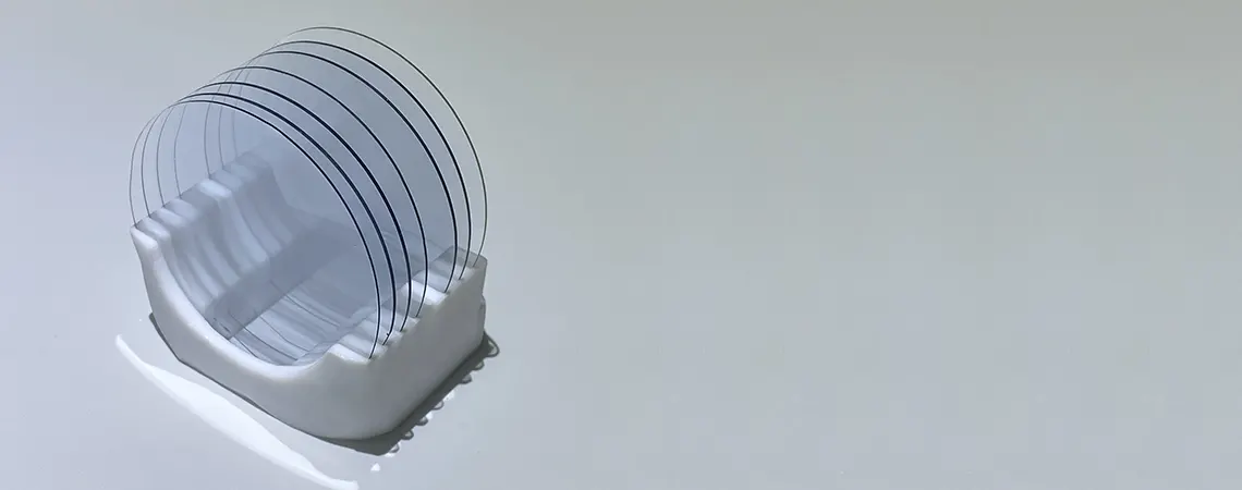
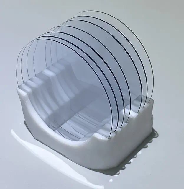
β-Ga2O3 Wafer
We provide β-Ga2O3products.
- 10×10 Ga2O3 Square Substrate
- 1インチβ-Ga2O3 Wafer
- 2インチβ-Ga2O3 Wafer
- 4インチβ-Ga2O3 Wafer
- β-Ga2O3 Seed Crystal


Gallium oxide is widely used in power electronics devices due to its high pressure resistance and low on-resistance characteristics. It has applications in electric vehicles, solar power inverters, high-speed railway power transmission, and has potential in other fields as well.
Gallium oxide has a band gap reaching up to 4.85eV and has excellent transmittance in the visible light spectrum. This makes it applicable in fields such as solar-blind ultraviolet detection and radiation detection.
Taking advantage of the low mismatch characteristics of gallium oxide single crystal and GaN, it is used for the growth of GaN for manufacturing high-performance high-frequency devices, which are expected to be applied in 5G communication.
10×10 β-Ga2O3 Square Substrate
| 10×10 β-Ga2O3 Square Substrate | |||
|---|---|---|---|
| Item | Specification | ||
| Crystal Orientation | (100) | ||
| Doping | UID | Sn | Mg/Fe |
| Nd-Na/Resistivity | 1016~1017cm-3 | > 1018cm-3 | ≥ 1010Ω·cm |
| FWHM (arcsec) | ≤150 | ||
| Dislocation Density | < 1×105 cm-2 | ||
| Size | A-B | C-D | Thickness |
| 10mm | 10.5mm | 0.5(±0.02)mm | |
| Reference | Long edge: [010] | ||
| Surface | Single-sided mirror / Double-sided mirror Ra < 0.5nm Crystal surface deviation < ±1° |
||
 |
|||
1 inch / 2 inch β-Ga2O3 Wafer
| 1インチ・2インチ β-Ga2O3 Wafer | |||
|---|---|---|---|
| Item | Specification | ||
| Crystal Orientation | (100) | ||
| Doping | UID | Sn | Mg/Fe |
| Nd-Na/Resistivity | 1016~1017cm-3 | > 1018cm-3 | ≥ 1010Ω·cm |
| FWHM (arcsec) | ≤150 | ||
| Dislocation Density | < 1×105 cm-2 | ||
| Size | Diameter | Thickness | |
| 25.4/50.8 ± 0.5mm | 0.65 ± 0.02mm | ||
| Reference | [010] | ||
| Surface | Single-sided mirror / Double-sided mirror Ra < 0.5nm Crystal plane deviation < ±1° |
||
 |
|||
4 inch β-Ga2O3 Wafer
| 4 inch β-Ga2O3 Wafer | |||||||
|---|---|---|---|---|---|---|---|
| Item | Specifications | ||||||
| Crystal Orientation | (100) | ||||||
| Doping | UID | Sn | Mg | ||||
| Nd-Na/Resistivity | 1016~1017cm-3 | > 1018cm-3 | ≥ 1010Ω·cm | ||||
| FWHM (arcsec) | ≤150 | ||||||
| Dislocation Density | < 1×105 cm-2 | ||||||
| Size | Diameter | Thickness | |||||
| 100.0 ± 0.5mm | 0.65 ± 0.02mm | ||||||
| Reference | [010] | ||||||
| Surface | Single-sided Mirror / Double-sided Mirror Ra < 0.5nm Crystallographic Misalignment < ±1° |
||||||
 |
|||||||
β-Ga2O3 Seed Crystal
| β-Ga2O3 Seed Crystal | |||
|---|---|---|---|
| Item | 仕 様 | ||
| Crystal Orientation | Long Side Direction (100) | ||
| Doping | UID/Fe/Mg | ||
| FWHM (arcsec) | ≤ 150 | ||
| Dislocation Density | ≤ 2×104 cm-2 | ||
| Size | A-B | C-D | Length |
| 4 ~ 7mm | 4 ~ 7mm | 30 ~ 100mm | |
| Surface | Cutting Surface Crystal Face Deviation < ±1 |
||
 |
 |
||