Wide-Gap Semiconductor Material Polishing
- Material
- SiC (Silicon Carbide), GaN (Gallium Nitride), Sapphire Wafers, etc.
- Specifications
-
2, 3, 4, and 6 inch wafers
- SBIR ≦ 1μm
- GBIR ≦ 2μm
- Ra ≦ 0.1nm or less
- Quality
-
Quality assurance by state-of-the-art inspection equipment
- Candela
- NIDEK
- AFM
- TXRF
- Edge Profiler
- Features
-
High flatness and heavy metal-free cleaning
- Substrate Polishing
- Backside Polishing of Epitaxial Growth Wafers
- Patterned Wafer Polishing (Planarization + Backside Polishing + Heavy Metal-Free Cleaning)
- Regeneration Polishing of Used Wafers
- Chamfering and Laser Marking
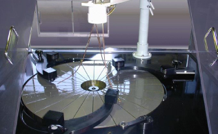
Lapping and Polishing Equipment