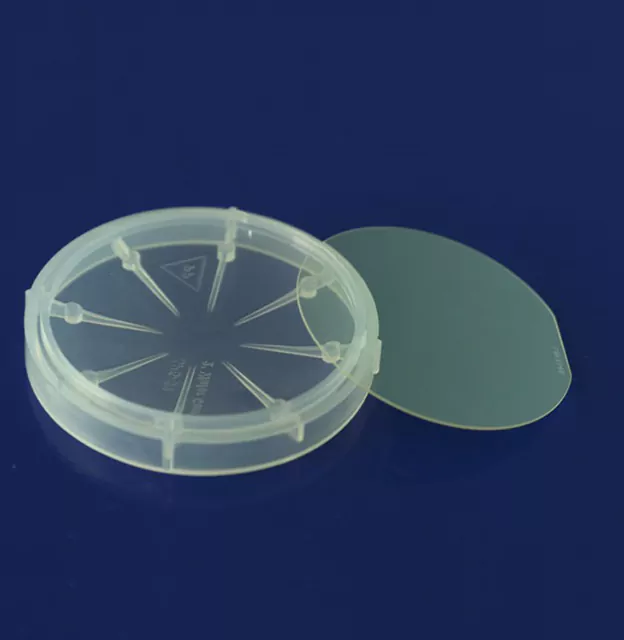
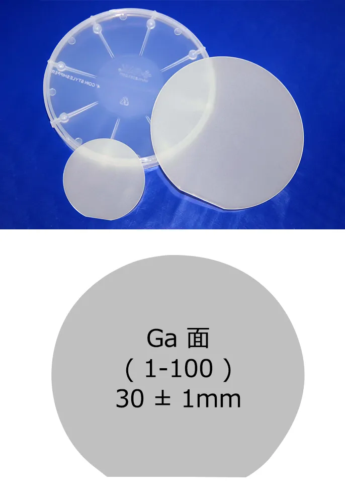
GaNウェーハ
GaNウェーハの製品を提供しております。
- 少量からのご注文
- パワーLSI、高輝度LED、レーザー用として注目
- 高品質(少ない結晶欠陥)
- 低価格(対他社比較)

パワーLSI用、高輝度LED用、高性能レーザー用に注目されています。
GaN基板

| 項目 | 仕様 | ||
|---|---|---|---|
| 直径 | 51.0 mm ± 0.3 mm | 100.2 mm ± 0.3 mm | |
| 厚さ | 490 um ± 30 um | 540 um ± 30 um | |
| 面方位 | (0001) Ga-face c-plane | ||
| TTV (5 mm edge exclusion) | ≤ 15 um | ≤ 30 um | |
| Warp (5 mm edge exclusion) | ≤ 20 um | ≤ 80 um | |
| Bow (5 mm edge exclusion) | -10 um to + 5 um | -40 um to +20 um | |
| 電気特性 | タイプ | 抵抗率 | |
| N-type (Silicon) | ≤ 0.02 ohm-cm | ||
| UID | ≤ 0.2 ohm-cm | ||
| Semi-Insulating (Carbon) | > 1E8 ohm-cm | ||
| グレード | Density (pits/cm2) | 2" (pits) | 4" (pits) |
| Production | ≤ 0.5 | ≤ 10 | ≤ 40 |
| Research | ≤ 1.5 | ≤ 30 | ≤ 120 |
| Dummy | ≤ 2.5 | ≤ 50 | ≤ 200 |
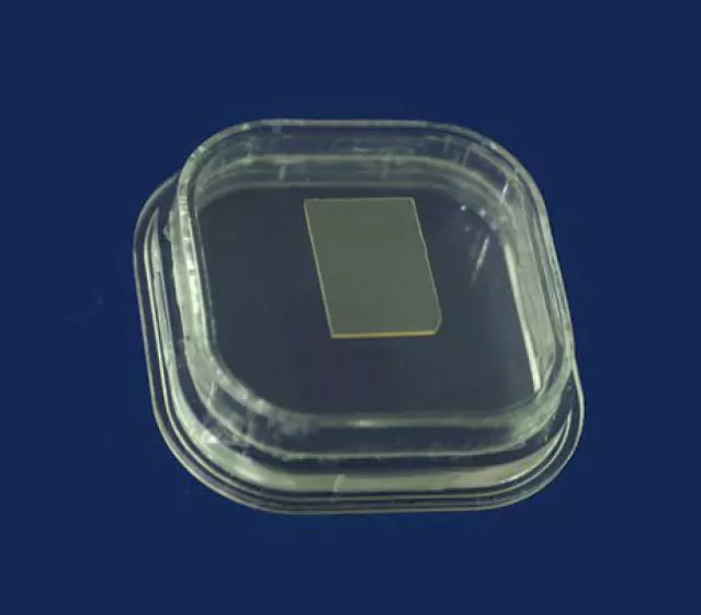
GaN基板(正方形)
| 項目 | 仕様 | ||
|---|---|---|---|
| サイズ | (10±0.5)×(15±0.5)mm² Customized Size |
||
| 厚さ | 400±25 μm | ||
| 面方位 | Cplane (0001)off angle toward M-axis 0.35±0.15°or 0.55±0.15° |
||
| TTV | ≤ 10 μm | ||
| BOW | ≤ 10 μm | ||
| 導電型タイプ | N-type (Un-doped) |
N-type (Silicon-doped) |
Semi-Insulating (Carbon-doped) |
| Ga face surface roughness | < 0.3 nm(10×10μm) | ||
| N face surface roughness | Etched(0.5~1.5μm);Polished(<0.3nm) | ||
| 転位密度 | < 1×106cm-2 | ||
| (002)FWHM | ≤ 70 arcsec | ||
| (102)FWHM | ≤ 70 arcsec | ||
| Macro defect density(hole) | < 0.3 cm-2 | ||
| 有効面積 | > 90% | ||
GaNテンプレート(φ2インチ)

| 項目 | 仕様 | |
|---|---|---|
| 直径 | φ50.8mm ± 0.1mm | |
| GaN膜厚 | 4um。 10~25um | |
| 方位面 | C面(0001)面 ± 0.5° | |
| 導電タイプ | N型 (Undoped) | N型 (Si-doped) |
| オリフラ方位。長さ | オリフラ方位(1-100)。 オリフラ長さ16 ± 1mm | |
| 電気抵抗率(300K) | < 0.5Ω・cm | < 0.05Ω・cm |
| 転移欠陥密度 | 5 × 10⁸ 個/cm2以下 | |
| 基板構造 | GaN / サファイアウェーハ(0001)面 | |
| 有効面積 | 90%以上 | |
| 表面仕上げ | Ga面:CMP仕上げ。 N面:ファイングランディング(オプション:光学鏡面仕上げ) | |
| 梱包方法 | クリーンルーム内にて窒素封入。1枚ごと梱包、又は25枚カセット。 | |
GaNテンプレート(φ4インチ)
| 項目 | 仕様 |
|---|---|
| 直径 | φ100mm ± 0.1mm |
| GaN膜厚 | 4um。 10~25um |
| 方位面 | C面(0001)面 ± 0.5° |
| 導電タイプ | N型 (Undoped) |
| オリフラ方位。長さ | オリフラ方位(1-100)。 オリフラ長さ30 ± 1mm |
| 電気抵抗率(300K) | < 0.5Ω・cm |
| 転移欠陥密度 | 5 × 10⁸ 個/cm2以下 |
| 基板構造 | GaN / サファイアウェーハ(0001)面 |
| 有効面積 | 90%以上 |
| 表面仕上げ | Ga面:CMP仕上げ。 N面:ファイングランディング(オプション:光学鏡面仕上げ) |
| 梱包方法 | クリーンルーム内にて窒素封入。1枚ごと梱包、又は25枚カセット。 |
4inch GaN-on-Sapphire Blue/Green LED Wafer

| Substrate | Type | Flat Sapphire | |
|---|---|---|---|
| Polish | Single side polished(SSP)/Double side polished(DSP) | ||
| Dimension | 100±0.2mm | ||
| Orientation | Cplane(0001)off angletoward M-axis0.2±0.1° | ||
| Thickness | 660±25μm | ||
| Epilayer | Structure | 0.2μm pGaN/0.5μm MQWs/2.5μm nGaN/2.0μm uGaN | |
| Thickness | 5.5±0.5μm | ||
| Roughness(Ra) | <0.5nm | ||
| Dislocation density | <5×108cm2 | ||
| Wavelength | Blue LED | Green LED | |
| 465±10nm | 525±10nm | ||
| Wavelength FWHMs | <25nm | <40nm | |
| Chip Performance | Cut-in voltage@1μA | 2.3-2.5V | 2.2-2.4V |
| Useable Area | >90%(edge and macro defects exclusion) | ||
| Package | Packaged in a cleanroom in a single wafer container | ||
2inch GaN-on-Sapphire Blue/Green LED Wafer

| Substrate | Type | Flat Sapphire | |
|---|---|---|---|
| Polish | Single side polished(SSP)/Double side polished(DSP) | ||
| Dimension | 50.8±0.2mm | ||
| Orientation | Cplane(0001)off angletoward M-axis0.2±0.1° | ||
| Thickness | 430±25mm | ||
| Epilayer | Structure | 0.2μm pGaN/0.5μm MQWs/2.5μm nGaN/2.0μm uGaN | |
| Thickness | 5.5±0.5μm | ||
| Roughness(Ra) | <0.5nm | ||
| Dislocation density | <5×108cm2 | ||
| Wavelength | Blue LED | Green LED | |
| 465±10nm | 525±10nm | ||
| Wavelength FWHMs | <25nm | <40nm | |
| Chip Performance | Cut-in voltage@1μA | 2.3-2.5V | 2.2-2.4V |
| Useable Area | >90%(edge and macro defects exclusion) | ||
| Package | Packaged in a cleanroom in a single wafer container | ||